NVIDIA Fermi: Architecture discussion

ninelven, 1/5 of Cypress is 544, not 272GFLOPS
no if you issue only one mul per clock then that's indeed 272 gflops (1/5 the instruction issue rate of fp32 mad only gets you 1/10 the flops cause those mads count twice as much...)

If my memory serves from the way it used to be in RV670 which first introduced DP on Radeons, basic add & substraction functions can be carried at 2/5 rate, while multiply and divide functions would go at 1/5 rate. (I doubt it has gone any worse from what it was back then)
you're right with add and mul (even with rv770), there's no divide (and no 64bit RCP). The 64bit FP mul on rv870 apparently only needs 2 of the slots and no longer all 4.
 
It has a read/write cache on the memory bus, very nice ... but that's not really a CPU style architecture. CPUs tend to be read/write and coherent across the entire cache hierarchy.
Almost CPU style caches then.
Because they have huge multipliers for DP around anyway, 50% of which will be idle when not doing DP ... no point in sweating the small stuff.
That must be one of the reasons why dp can't dual issue with anything else.
Have they even said they would do ECC on GDDR5?

Yup.
As we predicted previously, Fermi will have optional ECC support to protect data stored in memory, for both DDR3 and GDDR5, and the on-chip SRAM arrays are also protected.

The former is unsurprising, as DDR3 is designed for ECC from the start. However, ECC for graphics memory is much more interesting, as Nvidia’s engineers had to go above and beyond the GDDR5 specification to achieve that level of protection. Unfortunately, Nvidia did not disclose the algorithms and techniques used for ECC.
 
If you wrote your code using MADs, it had better produce the same results on all GPUs. Extra precision from FMA can be nice, but it can also be an unpleasant surprise.

Well, I think a 754R style FMA is better. Almost all CPU based FMA are of this style IIRC. They can have a compiler option (if you just want a global control) or even programming language directive (for fine tuned control) to make sure some corner cases do not use FMA by accident.
 
There seems to be a bit of confusion here about a number of things in terms of Fermi's execution units. I recommend this page of my article:

http://www.realworldtech.com/page.cfm?ArticleID=RWT093009110932&p=7

...

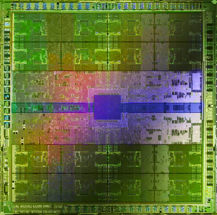
David, many thanks for the great article. Do you know what's at the very center of the die?

07.jpg
 
i skipped ahead a few pages and i am dead tired but i met Fudo at the little tri-private press conference where you get to talk to 2 senior Nvidia officials and they also do a presentation. It was supposed to last 1/2 hours (with a maximum of 1 hour allotted) but we kept asking questions - and they were eager to talk about Fermi - so it went way over. i got a lot clarified
. . finally i can set the record straight about "tesla" ..
it IS their architectural code name that CROSSED over into marketing .. and became a product like 'GeForce' or 'Quadro"
- But Firmi is a "first" in that the code name is being stressed by their marketing - because of the differentiation they want to make from the older series

GT 200 is GPU Tesla architecture 2.0
. . . So i want to apologize for backing down recently - after being right for well over 2 years; i got it right back then from a solid Nv source (clearly) and it still right! :p

Letsee, Fermi can be DDR3 but it is primarily set up for DDR5 on 384-bit.

Fermi definitely has TMUs and ROPs.
Yes, even more. They did go over the details; it is in their presentation to the press but i have to consult my note for accuracy .. later
I care about it's gaming performance.
Me too. They *guaranteed* it would be the fastest single GPU on release and they haven't given up on multi GPU nor X2 neither; ships '09.
 
Me too. They *guaranteed* it would be the fastest single GPU on release and they haven't given up on multi GPU nor X2 neither; ships '09.

Dont see why it wouldn't be. 240 cores>512 cores is a slightly bigger jump than 800 SP's>1600 SP's after all.

But we'll probably see a repeat of last gen, where ATI is a little slower but a lot smaller, too.
 
Makes sense, so presumably CUDA 3.0 / PTX2.0 will offer a mechanism for the developer to ensure that MADs remain as such?

Yes, it's called doing two operations instead of one. NV has no intermediate round, so you need to do an FMA that adds 0, followed by an FMA multiplying by 1. Not very nice.

Also, how does that work on RV870 which provides both MAD and FMA?

I don't know right now. They may have both unfused and fused operations.

David
 
Yes, it's called doing two operations instead of one.
Yes but there is only one DP instruction slot available per cycle ... so if for a moment we assume DP runs at 1/2 peak FLOPS of SP with FMA, it can not reach that with individual multiplies and adds. (Personally I don't think DP can reach 1/2 peak FLOPS of SP but that's a different matter.)
 
Why do they say that a SM has "8x the peak double precision floating point performance over GT200"? (Shouldn't that be 16.)

No, it should be 8x... Page 5.

Page 9- "up to 16 DP fused MADD ops can be performed per SM"
The graph of 4-4.2x DP App performance over G200.

Page 11- Table shows "256FMA ops/clock of DP", "512FMA ops/clock of SP".

http://www.nvidia.com/content/PDF/fermi_white_papers/NVIDIAFermiArchitectureWhitepaper.pdf

16ops x 16SMs x 2Flops x ~1600mhz = ~819GFlops which is ~8x the ~100GFlops of G200.
 
Here ... let me give the full context on their statement about 8x ...

Third Generation Streaming Multiprocessor (SM)
o 32 CUDA cores per SM, 4x over GT200
o 8x the peak double precision floating point performance over GT200
o Dual Warp Scheduler simultaneously schedules and dispatches instructions
from two independent warps
o 64 KB of RAM with a configurable partitioning of shared memory and L1 cache

Clearly by 8x there they meant performance of the entire chip at a conveniently chosen clockrate, how silly of me ...
 
Why does it have to be connected with frequency?

According to that thing for DP:

GF100 = 256 FMA ops/clock
GT200 = 30 FMA ops/clock

256 / 30 = 8.533333333333333333333333333 :LOL:
 
Why does it have to be connected with frequency?

According to that thing for DP:

GF100 = 256 FMA ops/clock
GT200 = 30 FMA ops/clock

256 / 30 = 8.533333333333333333333333333 :LOL:

You are right... Not necessarily connected to clockspeed.
I had this discussion elsewhere and before I reread the whitepapers I was going off what I remembered off the top of my head, which was 8x the DP of G200.
I found Nvidia's statement of ~100GFlops for G200 before I found that it can do 30DP ops/clock. :p
 
We have no details on the ATI 24-bit INT-MUL - is that just the 24 lowest bits? I suspect its for addressing type calculations.
What integer multiply? That's just the range of integers you can represent with a floating-point number without losing precision. You can do that with any single-precision IEEE 754 compliant multiplier. It has 23 mantissa bits and 1 sign bit (and 2 guard bits).

So extending this to 32-bit should be a relatively straightforward matter of adding a few more mantissa bits.
 
Back
Top