
You are using an out of date browser. It may not display this or other websites correctly.
You should upgrade or use an alternative browser.
You should upgrade or use an alternative browser.
NVIO specifications?
- Thread starter hkultala
- Start date
I think the difference would be minor (a few mm²?). One of the key benefits of NVIO isn't die-size reduction (I think), but yields and manufacturing price. Defect in I/O section would kill entire 500mm² GPU. SPs, TMUs, ROPs and MC can be switched of and GPU can be sold as a cheaper part, but I/O abilities are essential.
I'm curious, if the yields and price benefits of the NVIO are still present during current aggressive price war - e.g. it can be good to invest a few more $ to rescue some GPUs, which can be sold for price X, but is it still profitable, if you must sell these GPUs for price X/2 or X/3?
I'm curious, if the yields and price benefits of the NVIO are still present during current aggressive price war - e.g. it can be good to invest a few more $ to rescue some GPUs, which can be sold for price X, but is it still profitable, if you must sell these GPUs for price X/2 or X/3?
I actually have related question.
If nVidia had included NVIO-features into G80 and GT200 instead of separate chips, how much would it have grown the chip in terms of transistors and/or diesize?
Not much, BUT
they already have huge number of pins because of wide memory bus, and replacing the few pins of the "nvio link" with all the connections that nvio offers would have increased the pin count quite much, and made the PCB even more expensive.
G92 got rid of separate nvio bus not because of mfg process/die size, but because of anrrower 256-bit memory bus.
Certainly not the last two options.I've read these numbers till now: 231mm², 264mm², 270mm², which is true ?
")
I don't think this is correct. Couldn't find many real measurements (most of the die size information you can find is just quotes from unknown sources), but one site measured it at 265mm². Using same method they got 275mm² for rv770. http://www.pcgameshardware.de/aid,6...200-und-GT200b-nachgemessen/Grafikkarte/News/~230mm²
@fellix,
270mm²:
http://www.xbitlabs.com/articles/video/display/palit-gf250gts_2.html
http://forum.beyond3d.com/showpost.php?p=1174757&postcount=3251
268mm²:
http://www.yougamers.com/forum/showthread.php?t=82833
264mm²:
http://www.hardforum.com/showthread.php?t=1325165&page=2
~230mm²:
http://www.tomshardware.com/reviews/geforce-gts-250,2172-2.html
http://www.hardforum.com/showthread.php?t=1325165
That's why I am confused
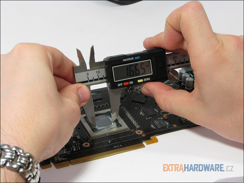
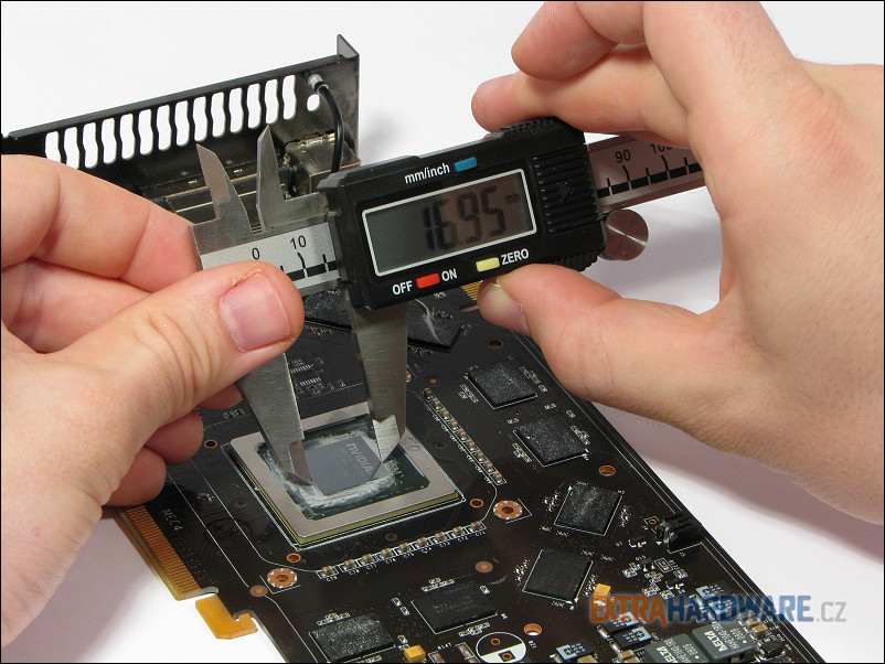
From our excel sheet
NVIO 1 6,2 6,1 37,82mm²
NVIO 2 5,85 6,17 36,0945mm²
(measured, son including some margin of error due to packaging)
How much of this is because of packaging and padding, how much for the actual die functions?
I think hkultala is talking about something different. It's likely, that only a fraction of the die is used for RAMDACs and TMDS - the rest is present only to reach dimensions necessarry for I/O pads. Notice, that despite different manufacturing proces, both dice versions are about the same size.
Similar threads
- Replies
- 52
- Views
- 5K
- Replies
- 18
- Views
- 2K
- Replies
- 242
- Views
- 19K
- Replies
- 115
- Views
- 12K