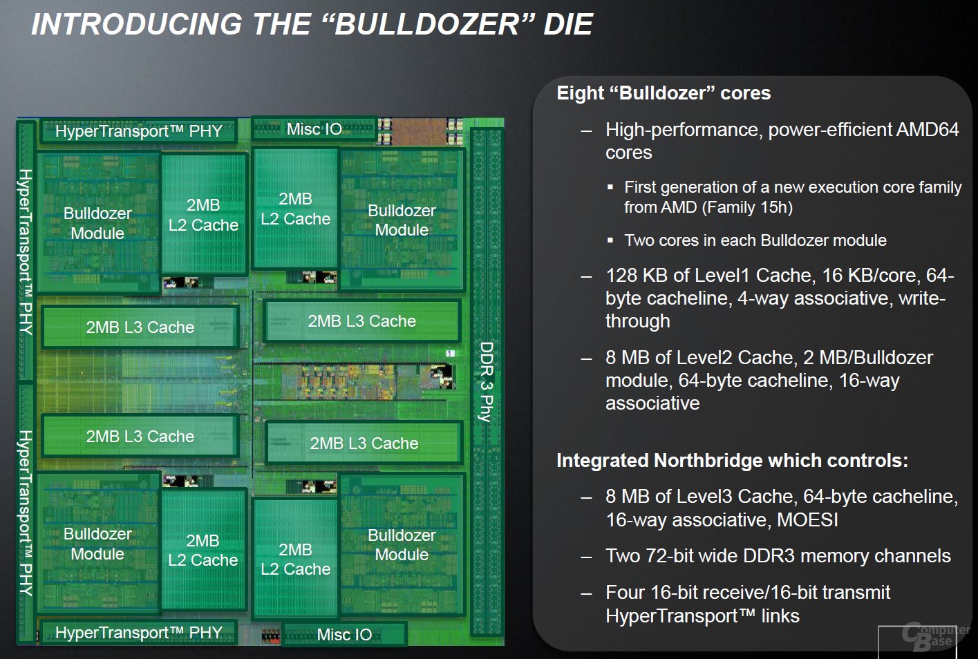
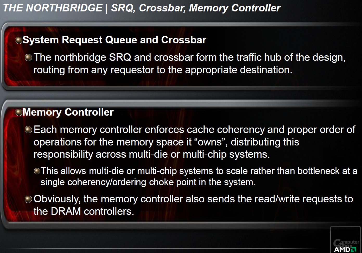
AMD Bulldozer Core Patent Diagrams

Game testing in heavy CPU limited scenarios (such as those low resolutions) is purely academical, I wouldn't worry too much about that. However, those numbers look a bit low for a part that was supposed to turbo @ 4.2+ Ghz, maybe it easily gets TDP limited.

I wouldn't say it's academic. It may be when the framerates are so high but there are plenty of games which need a lot of CPU power these days and if that requirement keeps going up (which it will) the weaker CPU in todays academic tests is the CPU that is too slow to play tomorrows games.
 
No doubt. My current CPU is 3.5 yrs old and will be close to 5 before upgrading. A 3-5 year cycle for CPUs is more than sufficient nowadays for gaming.
 
Wow, this thing really looks like a turd.

If B3D ever interviews an AMD CPU engineer, I think an apt question would be "Why do you continue to produce turds?"
 
Wow, this thing really looks like a turd.

If B3D ever interviews an AMD CPU engineer, I think an apt question would be "Why do you continue to produce turds?"

Please, try to design your own multi-gigaherz, multi-pipeline OOE processor which still has to have full SW compatibility to quite quirky 30 year old processors.

When you have done this, you may have an answer to your question.


And.

Bulldozer has not been released. We have seen NO benchmarks which give results we can trust. We have seen "leaks" and fakes, some numbers completely made up and some numbers run with beta-hardware which have had some performance-improving features off, and clock speeds have also been lower than final hardware.

Lets wait until we have some number with the real final hardware, running at final clockspeeds, until making any stupid judgements.
 
I really hope Bulldozer do great thing, we need a good AMD in the CPU market. Can't wait for "true" benchmarks.
 
The fx-8150 is slower than the phenom II x6 at 3.3ghz.
Other than the game results the BD is right up there with/beating the top-end Intel CPUs in those scores & well out ahead of Phenom IIs.
This is looking generally pretty good I think.
 
Sad revelations from a former AMD CPU engineer:
The team that did all the great design work for Athlon 64/Opteron is gone. Forced out or quit in disgust. They now work at Apple, Oracle, misc. startups, and, in my case, changed careers.

...The team that designed the K6-2 was the CMD team, which was formed by the acquisition of a company called Nexgen. That team also designed Athlon 64 and Opteron (Athlon was designed by the TMD team). By 2007, all the key CMD folks were gone. The team that was left sucks, and has accomplished little since then other than shrinks to smaller technology and bolting more of the same cores on

....Yeah. Like replacing the 40-man team that designed A64 with a 250 man team for minor design changes. And like throwing away all the EDA tools because the vapor tools from the texas design team would be better if they ever were finished....

The new CEO [Dirk Meyer] is a guy that once told the design team (when he was a manager in Texas) "if you don't like it, quit" - and 60 out of 100 people in Sunnyvale quit within a month. They used to hand place and hand instantiate each cell in the design for maximum efficiency and speed - now they rely on tools which perform 20% worse than humans (in order to save money). ..
.


Guys - I have nothing to be disgruntled about. I left on my own accord. I had great times at AMD making a64 and creating amd64. AMD paid me enough to pay for a house in silicon valley and a porsche. I quit on my own and was not pressured to do so. They were sad to see me go, and i was sad to leave
...
I am not disgruntled. I am sad. Sad that AMD squandered their lead because new management decided that the way to compete was design CPUs the way that chips in toasters are designed. And worse, to do it with giant teams of unskilled designers instead of a small team of highly experienced engineers who know how to design transistor by transistor. ....


And the biggie on how Hector's Fusion strategy stabbed the remaining carcass:

.What did happen is that management decided there SHOULD BE such cross-engineering ,which meant we had to stop hand-crafting our CPU designs and switch to an SoC design style. This results in giving up a lot of performance, chip area, and efficiency. The reason DEC Alphas were always much faster than anything else is they designed each transistor by hand. Intel and AMD had always done so at least for the critical parts of the chip. That changed before I left - they started to rely on synthesis tools, automatic place and route tools, etc. I had been in charge of our design flow in the years before I left, and I had tested these tools by asking the companies who sold them to design blocks (adders, multipliers, etc.) using their tools. I let them take as long as they wanted. They always came back to me with designs that were 20% bigger, and 20% slower than our hand-crafted designs, and which suffered from electromigration and other problems.

That is now how AMD designs chips. I'm sure it will turn out well for them [/sarcasm]
Source: Macrumors forums, via [H]
 
The [H] post is recent, the links it reposts are old, and I'm pretty sure these have come up before.

AMD's shift to a more automated flow, and the consequences of that choice have been admitted.
BD's stripped down cores and longer pipeline basically keep it in place in a world where it does not seem to believe it can count on a having money, which includes subsidiary assumptions that it may not have as good a process or as heavily customized logic.

The speed racer design in BD probably saw some of its theoretical clock eaten up by these details.
Fusion designs have a dominant part of their logic taken up by an ASIC.


It may be interesting to see if Maier's analysis is as relevant now as it was during his tenure.
One question is that AMD looks to be positioning itself to be a second-fiddle value proposition, so could it sustain the style of design he espoused, as design complexity increases?

Another is the question of the payoff for that heavy level of engineering he is writing the eligy for.
Are the benefits as significant at current and upcoming nodes as they were back in the K8 days, and are the costs any higher?
 
bulldozerdiesize1.png


The official die-size is confirmed at 315 sq.mm. Not much different from what was speculated already.
The six core 32nm Gulftown die is 32% smaller, for comparison.
 
I don't really understand dies, but it seems to me that there is a whole lot of empty space in that picture? Why would they make it like that if that is the case?
 
There's some slight detail in the empty space in the center. There's probably miscellaneous logic in there that either didn't show very well or AMD made sure did not show well.

At least some of it could be IO controllers and the interconnect between the modules and L3 partitions.
The ring of blank space around each module could be attributed to the power gating transistors.

I need to go over what SB and BD dedicate for uncore area when I have the time to see if one or the other is more area-efficient.
 
bulldozerdiesize1.png


The official die-size is confirmed at 315 sq.mm. Not much different from what was speculated already.
The six core 32nm Gulftown die is 32% smaller, for comparison.
You're speaking of the Orochi "4 modules / 8 cores" thingy? That's damned huge :oops:

EDIT found the picture at semiaccurate. It's still damned big.

EDIT OK the picture was blocked at my job but usually I've something stating so.
 
Last edited by a moderator:
There's some slight detail in the empty space in the center. There's probably miscellaneous logic in there that either didn't show very well or AMD made sure did not show well.

At least some of it could be IO controllers and the interconnect between the modules and L3 partitions.
The ring of blank space around each module could be attributed to the power gating transistors.

I need to go over what SB and BD dedicate for uncore area when I have the time to see if one or the other is more area-efficient.
There is a cross-bar interconnect wiring between the L3 slicesright in the middle of the die, but it's still considered a waste. SNB, for example, routes its ring-bus wires beneath the transistor logic, and I guess this is due to more robust hand tuned layout, where AMD cut some corners with automatic placement process.
 
A crossbar is also physically more complex and can be more congested than a more straightfoward ring bus.
In Intel's case, I think the ring bus goes over the L3 cache slices, not the logic.
Intel's distributed ring bus protocol would also not be sufficient for AMD's crossbar, so more centralised arbitration logic could take up space in that section as well.

Given the higher complexity, there may have not have been room to put all the wires over the cache.
 
I haven't seen many details on the BD crossbar. It seems possible AMD's crossbar could be more capable than Nehalem's, given the server focus of BD.

It does look like Intel does devote a measurable amount of die space in the middle of the L3 to some kind of logic for the interconnect.
It does seem plausible that Intel could engineer more area savings than AMD in this regard, though it does seem like the ring bus takes up less room than that.
 
The dual die Interlagos CPU-s will face each other probably trough the side with HyperTransport phy. Could it be that the area till the northbridge is actualy there for the two chips comunication.:?:

Edit: Or just with the aggressive clock gating its the safest place for the wiring.
 
Last edited by a moderator:
Clear shot from the slides.
4.jpg


Basicly its more server oriented than sandy bridge. Probably the server margins can justify the die size increase in consumer parts.

12.jpg
 
Back
Top