PCGH - Pixelshader-Shootout: RV770 vs. GT200

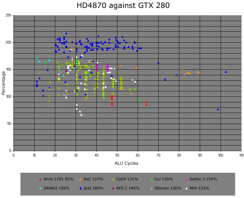
Some NVidia comparisons, too:

Code:
GTX280 faster than   GTX260 8800U
GRAW 2               95%    114%
Rainbow Six: Vegas   97%     97%
Call of Duty 4       98%    112%
Gothic 3             99%    107%
Anno 1701            97%    112%
Test Drive Unlimited 97%     96%
Call of Juarez       98%    104%
Race Driver Grid     97%    112%
Oblivion             97%    105%
Stalker              97%     98%
Age of Conan         97%    110%
NfS Most Wanted      97%    104%
NfS Carbon           96%    106%
Average              97%    105%

So the scaling for GT200 is pretty close to theoretical. GT200 v G80 is all over the place, so I guess the prodigal MUL could be doing something...

Jawed
 
Please disregard the results from GRAW2 and RB6 Vegas - those were the games having obvious trouble with some of the MRT-heavy shader and thus not included in the article.

Some individual and erroneous results showed a GTX280 to be about 20 times faster than HD4800 - so a pretty obvious error.

For comparisons strictly within one family however, they could eventually be used.
 
OK, so I've got the PCGH raw data :cool:

I notice some of the shaders are SM1.x. I think the instruction limit is 8 instructions for SM1.0, 1.1, and 1.3:

http://forum.beyond3d.com/showthread.php?t=3312

but it appears to be 16 instructions for 1.4.

So is it reasonable to assume that all SM1.0, 1.1 and 1.3 shaders are fillrate limited on HD4870, which can execute 10 ALU instructions per clock per pixel :?:

Unfortunately some shaders are described as 1_x, so I'm not sure if that means that they could be 1.4.

The first thing I'm going to do is a histogram of all the fillrates for each card. I think this should show peaks for 1, 2, 3 and 4-colour output from the shaders. If so, then I should be able to classify shaders that fall within a small percentage of the 2, 3 and 4-colour peaks as being fillrate-limited. The peaks, when scaled by clocks within an architecture (e.g. HD4870 + HD4850 as one architecture, GTX280 + GTX260 as another) should line up. NVidia's separate core and ALU clocks should help too.

A brief look at the data seems to indicate that some ATI fillrate limited cases are a bit strange, e.g. 11399 G pixels/s on HD4870 and 6085 on HD3870 (instead of ~11800). Do these GPUs vary in fillrate for one or more formats of render target? fp16? fp32? int32? ~6090 appears to be quite common in the set of HD3870 fillrates, so it does appear to be a fillrate limited scenario.

Of course it could be coincidence, after all HD4870 can be fillrate limited when HD3870 isn't.

Anyway, for the purposes of a scaling comparison of HD4870 and GTX280, I'm trying to identify all shaders that are fillrate limited on either GPU. I'm puzzled why PCGH didn't exclude these cases from their analysis originally, since it's so clear from the data just how often fillrate is the bottleneck. Maybe it was just a question of time to sift through this wodge of data :oops:

Jawed
 
Please disregard the results from GRAW2 and RB6 Vegas - those were the games having obvious trouble with some of the MRT-heavy shader and thus not included in the article.
Carsten, it seems Stalker is the same. See shaders: 3_0: 3, 4, 7, 11, 13, 16, 22, 23, 30. These are all way faster on 8600GTS than HD4870 :p

There's a couple of Gothic3 shaders that are doing the same, too.

Out of 4949 shaders across 13 games, I've disqualified 3493 shaders due to being fill-rate limited on HD4870, having a fillrate of 0 or being from a disqualified game (GRAW2, R6V, Stalker). Note that R6V accounts for 1232 of the excluded shaders!

Ranges on HD4870 that seem to be fillrate limits, in M pixels/s with count:

Code:
   Range     Count 
11290-11530    773
 7782-7800     261
 5871-5885     423  
 4712-4723     522
 3935-3945     522
 2959-2967     309
 2634-2640     210

Each of those ranges, apart from the top one, has a very small spread, ~0.25%.

I haven't worked on GTX280 fillrates much.

Jawed

HI Jawed,

The "0" shaders were not part of the calculated total - they were taken out of the overall sums and the dividers accordingly diminished and the games containing it taken out of the graphs on the english article. edit: Seems like, deferred renderers are a the primary cause of grief for our tool. :(

Obviously, I have missed the Gothic 3 case - maybe because it's overall picture was roughly in line with the expected results comparing GTX and HD48.


We didn't exclude fillrate limits, because we wanted to average on a workload as close as possible to what real games are using - and in turn identify where possible bottlenecks are. To be more precise: That was exactly one of the points of our test compared to purely synthetic benchmarks like Rightmark 3D, Shadermark or Xbitmark.

Of course, we do know that the HD4800 commands vastly superior ALU horsepower but nevertheless does not come out victor in some/many/most (depending on which results you look at) game tests.


Since we do not know whether or not the fillrate bottlenecks are there with original texture looksups and the like, we cannot say for sure but at least take an educated guess as to whether it was a good idea to put this much ALU-horsepower into a chip with a color-fill limit of 'only' 12 GPix/s.

If we assume for a moment that 'small texturing' does not provide GT200 with an unnatural large boost (which I'd strongly think, since there's more TEX per ALU on the Nvidia side of things), these results do seem to be explaining the situation quite a bit.
 
Last edited by a moderator:
Since we do not know whether or not the fillrate bottlenecks are there with original texture looksups and the like, we cannot say for sure but at least take an educated guess as to whether it was a good idea to put this much ALU-horsepower into a chip with a color-fill limit of 'only' 12 GPix/s.
Certainly the deferred rendering case is an interesting question.

If NVidia's next architecture is GDDR5 based and only has 256-bits and only 16 pixels per clock of colour fillrate, things will definitely not be pretty - if colour fillrate is important.

You've alluded to problems with your test setup that arise due to MRTs (which sounds as if NVidia's driver is altering the render state when it discovers that only one target is getting consumed after it's generated). Can you tell from the shader code that you've captured which shaders are writing to more than one target?

One of the things that I'm wary of in removing HD4870's fillrate limited shaders is that it's quite possible for a shader to be simultaneously ALU and fillrate limited - it merely needs to run for 10 ALU cycles with one colour write, for example. So far I haven't thought of a way to separate the ALU limited case (10 or more ALU cycles per pixel) from the fillrate case.

Comparing HD4870 and HD4850 I find 6 cases of apparent bandwidth limitation:

Code:
Game       SM  ShaderID  HD4870  HD4850  Ratio
Anno 1701 1_1   31       94.4    86.3    109
AoC       3_0   83       95.9    87.5    110
CoJ       3_0  157       32.9    31.0    106
Oblivion  2_x  109       32.8    30.7    107
RB6V      3_0  200       39.3    36.7    107
RB6V      3_0  278       32.8    30.5    108

The two GPUs' fillrates are stated in terms of theoretical maximum, e.g. 16*750MHz for HD4870.

Jawed
 
A summary of where I've got to so far:

b3da018.png

Overall, HD4870 is 145% of the speed of GTX280.

"ALU Cycles" is calculated as the theoretical fillrate divided by achieved fillrate and then multiplied by 10, since HD4870 has a 10:1 ALU:fragment ratio.

This is a set of 519 shaders across 10 games. I've drawn up a number of rules to identify results that are suspect, and therefore rejected, from the set of 4949 total game shaders. A lot of the rules are based on intra-family performance scaling, e.g. HD4870 against HD4850 or HD3870. I've been both too lenient in some cases and too strict in others, which is why the longest shader is only 103 cycles (1170MP/s on HD4870 and 802MP/s on GTX280). I'll prolly spend more time on the rules at some point, particularly as I suspect there are plenty of long shaders that shouldn't be excluded (e.g. some Oblivion shaders appear to be pretty long, e.g. 253MP/s on GTX280 which runs at 625MP/s on HD4870).

Jawed
 
why does the ati card have so much theoretical math power, but in games its not showing up ?
going by the chart CarstenS put up
 
Bandwidth or texturing limits, I'd guess. Math isn't the bottleneck. Although I have seen a few reviews where the 4870 is beating the GTX 280.
 
I'm sorry Jawed, but that is about the butt ugliest graph I've ever seen and I don't understand it. :???:

EDITED BITS: Lemme rephrase that as it's been pointed out to me that my post was more disparaging than I intended....

Thanks for taking all the time and effort in making the graph Jawed, but I really don't get it. Could you please explain a bit in what it shows?
 
The thread discusses why PCGH's graphs are mostly not about ALU evaluation.

A very significant proportion of all the shaders tested (4949 shaders) are in some way fillrate limited. And because of PCGH's testing arrangement, some of these fillrate-limited shaders are not actually fillrate limited in games. Other shaders show other reasons, potentially due to bandwidth or other factors I can't identify.

So I have spent a while devising rules to exclude shaders based on various performance comparisons, whether fillrate limitation or to do with "incorrect" scaling within families (or in some cases scaling across families).

So I'm left with 519 shaders that are genuinely ALU-limited (though there may be 10-20 that aren't). The net result is that HD4870 is 45% faster than GTX280. On the basis of theoretical FLOPs, HD4870 is 29% faster than GTX280.

NVidia's "scalar architecture" is certainly not more efficient on average. And that's before taking into account that GTX280's ALUs consume over twice the die space of HD4870's, though there is a process gap playing its part.

---

One of the issues with these shaders is there's no way to tell what proportion of frame rendering time is represented by each shader. e.g. the slowest shaders might only run for a few thousand pixels per frame on average.

---

Overall, few games are genuinely limited by ALU performance. Grid is prolly the first game that shows a marked ALU-limitation:

http://www.anandtech.com/video/showdoc.aspx?i=3415&p=7

Here the 1GB HD4870 is 29% faster than GTX280. The results I posted above for Grid are based on 132 shaders, which average 83% faster than GTX280. The full game has 372 shaders according to the data Carsten gave me.

Jawed
 
Could you please explain a bit in what it shows?
See the blue triangles? That's the 132 different shaders for the game Grid that I've identified as likely to be genuinely ALU-limited shaders.

These 132 shaders average 83% faster on HD4870 than on GTX280.

The second-slowest shader, about 98 ALU instruction cycles, is slower on HD4870 than GTX280. This shader runs at about 77% of the speed it runs on GTX280.

The slowest shader, about 103 ALU instruction cycles, is ~45% faster than on GTX280.

The best case for HD4870 is about 117% faster than GTX280. This shader is about 25 cycles.

There are no shaders of 10 or less cycles on the graph because 10 is the fillrate limit for RV770.

Jawed
 
Hi Jawed,

Sorry for not having any more time to discuss this topic with you beforehand, but work did quite occupy me the last few weeks and now I'm already on vacation. :)

Thanks for taking the time and reshuffle and select the data anew to draw a different conclusion. Interestingly, you come with about 45% more performance for HD 4870 over GTX280 - which is somewhere in between the marketed max. GFLOP-Ratings for both chips (3/ALU/cycle for GT200 which i tend to dislike) and the more achievable number of 620ish GFLOPs for it if only counting 2 FLOPS/clk.

Our goal, however, was not to take only ALU-limited cases into consideration but deliberately use a wide range of shaders used in actual games.

But it's great to see our data put to use once more to analyze RV770 and GT200 from this point of view.
 
Interestingly, you come with about 45% more performance for HD 4870 over GTX280 - which is somewhere in between the marketed max. GFLOP-Ratings for both chips (3/ALU/cycle for GT200 which i tend to dislike) and the more achievable number of 620ish GFLOPs for it if only counting 2 FLOPS/clk.
I really see no reason not to count GT200 as MAD+MUL, i.e. 933GFLOPs.

If you want to count just the MAD, i.e. 622GFLOPs by ignoring the multifunction interpolator (interpolation, transcendental, MUL), then you should also discount the transcendental ALU in RV770, i.e. make it 960GFLOPs.

That makes RV770 theoretically 54% faster than GTX280.

NVidia's architecture overloads the ALUs with attribute interpolation. I don't see how we could account for this, since it varies by shader. If we take the two longest Grid shaders, 98 and 103 ALU cycles on RV770, is it reasonable to suppose that either of these is attribute-interpolation bound on GTX280?

In theory it's possible to heavily reduce throughput on GTX280 by making a pixel shader compute a function of 2 or more attributes, requiring all the interpolations to be done first.

Without seeing the code of the shaders, though, it's not possible to go much further.

There's no accounting for immaturity in NVidia's compiler. Arguably, compilation for MAD+MUL is "new" for NVidia on this architecture. On the other hand, this is an architecture that should have been up and running back in late 2007, even if it wasn't ready for consumer release.

Separately the increased register file size in GT200 may be showing up immaturity in the compiler, as the allocation of warps versus shader complexity (register count) is different again.

In the past I've linked this patent document:

Dynamic instruction sequence selection during scheduling

which suggests that:

[0004] Because a low level language may include complex instructions that perform a combination of functions, there is the possibility of performing an identical operation using two ore more equivalent instruction sequences. In the example provided above, a multiply and accumulate operation can be scheduled as a single MADD instruction or alternatively as separate multiply and add instructions.

[0005] Thus, many times a particular computation in an application can be compiled in multiple ways, using different instructions or sequence of instructions. Traditionally, the selection of instruction sequences corresponding to the computation is performed prior to the scheduling of instructions. However, in many cases, it is not possible to determine a priori which instruction sequence results in an optimal schedule for a given program.

[0006] The alternative instruction sequences that correspond to the same computation may utilize different hardware resources. A particular processor configuration can have multiple execution units and the execution of particular instructions may or may not be constrained to particular execution units. For example, some instructions may be limited to execute on specific execution units within a processor, while other instructions may be executed by any of a number of execution units.

[0007] The hardware constraints associated with particular instruction sequences further complicates instruction selection and scheduling. In some cases, it may be beneficial to use an instruction sequence that uses specific resources. In other cases, it may be beneficial to use an alternative instruction sequence that utilizes other machine resources. For example, in one case, it may be beneficial to select and schedule an instruction sequence that reduces dependency depth. In another case, it may be preferable to schedule an alternative instruction sequence for the similar computation because the alternative instruction sequence reduces the register pressure.
So it may simply be a matter of time for NVidia to refine the costing models inside the compiler.

The final factor, one that's often missed, is that HD4870's transcendental throughput is 54% higher than GTX280's. This is a lot higher than the 29% based on pure theoretical GFLOPs. I'm still in the dark as to whether any graphics transcendentals are "half speed" on GTX280, as there seems to be cases of half speed for CUDA transcendentals...

Jawed

Where did you get this 54% figure? Because I just recently tested with GPUBENCH (instrissue) and what struck me that the transcendentals were only slightly better than the archived 8800 GTX results, but the other arithmetic tests were significantly faster.

I tested with a 4870 X2 though, but that should yield similar results to a 4870.

BTW, would one reason for the supposedly low utilization of the extra MUL on Nvidia be that the actual code doesn't have proportionally so many MULs? To achieve maximum utilization on Nvidia, you should have twice as many MULs as ADDs. With an equal proportion like with ATI, utilization _might_ be better.
 
Where did you get this 54% figure?
HD4870 has 10 clusters * 16 transcendental ALUs * 750MHz = 120G transcendentals per second, while Nvidia has 10 clusters * 3 multiprocessors * 2 transcendental ALUs * 1296MHz = 77.76G transcendentals per second.

BTW, would one reason for the supposedly low utilization of the extra MUL on Nvidia be that the actual code doesn't have proportionally so many MULs? To achieve maximum utilization on Nvidia, you should have twice as many MULs as ADDs. With an equal proportion like with ATI, utilization _might_ be better.
Yes. NV40 suffered in a similar way, which was improved in G70 by making both ALUs MAD. I think it amounted to ~30% extra performance on some synthetic tests.

Jawed
 
which was improved in G70 by making both ALUs MAD.

MAD They're bloody furious....

but on a more serious note, with nvidia allegedly helping to get physx running on ati hardware, if it did run would ati be kicking some serious ass ?
 
but on a more serious note, with nvidia allegedly helping to get physx running on ati hardware, if it did run would ati be kicking some serious ass ?

I suppose that since Havok is free for use and ATi said that they are gonna support it in their hardware and Intil is also going to support it obviously the future for PhysX could get pretty grim ;) On the other hand I don't really see them pushing results or anything on the table so may be they are just hoping that the mere rumor of support of PhysX on ATi cards will encourage more companies to use it. As with most things NVidia it's more about advertising than actually doing something ;) (I mean what happened with the Big Bang II in september :rolleyes:) Also if done "properly" the phisics acceleration on the Radeons could end up slower ;)
 
Back
Top