
You are using an out of date browser. It may not display this or other websites correctly.
You should upgrade or use an alternative browser.
You should upgrade or use an alternative browser.
The Future of the Playstation
- Thread starter Color me Dan
- Start date
EDRAM barely makes sense this generation, it will make even less sense in the next one, unless GPUs will radically change their compositing model (but this is not going to happen, imho)
Hey, now I can ask a question I have had for you

What solutions do you propose?
On the GPU side we continue to see bandwidth needs increase with IHV's up to 384bit and 512bit memory buses. It seems, from a console perspective, we would be lucky to see a 256bit bus in the new consoles.
On the other side of the MB you have the CPU, which is also increasing in cores. I know Intel is expecting to have a wide number of memory controllers embedded.
So we may continue to see an increase in GPU bandwidth needs (maybe not as much... but where is the cap where it begins to level off? Any suggestions nAo?) and on the CPU end we will see bandwidth needs increase both with core increases as well as clock increases.
So what should be done about it?
Split pools? That hasn't been popular and could be costly. A unified pool is nice, but you could have some serious client contentions. A unified pool with an eDRAM scratchpad for certain tasks?
Other?
I am really interested to hear the solutions you think future consoles could employ. You have proven quite capable of finding elegent solutions in place of brute force hardware approaches, so I would venture you have something in mind
EDRAM barely makes sense this generation, it will make even less sense in the next one, unless GPUs will radically change their compositing model (but this is not going to happen, imho)
Why? Having dirt cheap alpha and free pixel side msaa is quite helpful. Alpha to coverage, or rendering large alpha surfaces at low res like they were suggesting at PS3Devcon doesn't cut it in many cases, especially when you need to preserve texture detail. Being able to support lots of overdraw (for certain effects) is also very helpful. Plus it's not like we're gonna see another jump in resolution next generation, so it should be possible to get enough edram in there to avoid tiling in a few years.
Nothing completely new, just bandwidth compression, and maybe something a bit more exotic..What solutions do you propose?
Don't forget that we will also have faster memories.On the GPU side we continue to see bandwidth needs increase with IHV's up to 384bit and 512bit memory buses. It seems, from a console perspective, we would be lucky to see a 256bit bus in the new consoles.
That's another reason why I don't see EDRAM happening next gen; CPU and GPU will be even more close than they are now, possibly sharing more resources.On the other side of the MB you have the CPU, which is also increasing in cores. I know Intel is expecting to have a wide number of memory controllers embedded.
I don't believe there's a cap, bandwidth requirements will indefinitely go up and up..So we may continue to see an increase in GPU bandwidth needs (maybe not as much... but where is the cap where it begins to level off? Any suggestions nAo?) and on the CPU end we will see bandwidth needs increase both with core increases as well as clock increases.
Given the fact that an unified pool is more desirable but not always attainable, I expect next gen console to mostly use unified pools, simply cause CPU and GPU will get someway together or very close architecture wise. They will need to cooperate more and more..So what should be done about it?
Split pools? That hasn't been popular and could be costly. A unified pool is nice, but you could have some serious client contentions. A unified pool with an eDRAM scratchpad for certain tasks?
Though I don't see them on the same chip, unless we are talking about some kind of next gen underpowered console (Wii2)
The problem is that is not dirty cheap from a manufactoring stand point, and unless tomorrow we will have some kind of edram that is easy to embed with logic on the same die I think it's not worth the hassle (Arun don't cite zram!joker454 said:Why? Having dirt cheap alpha and free pixel side msaa is quite helpful.
)As I already proposed many times on these forums for all the stuff you're worried about there's imho a relatively simple solution: small on chip buffer + wide internal bus + (CPU)tiling.Alpha to coverage, or rendering large alpha surfaces at low res like they were suggesting at PS3Devcon doesn't cut it in many cases, especially when you need to preserve texture detail. Being able to support lots of overdraw (for certain effects) is also very helpful.
Supporting 32x32xmaxAA tiles on chip would be pretty amazing, I'd use something like that for all the bandwidth heavy compositing (particles or other fancy effects).. to be honest one could implement the last part of the REYES rendering pipeline with that..
For example supporting 128bits per pixel render targets + zbuffer + 8xAA would take just 160k on chip, probably an awfully small area on 32 nm chips (the difference here is that this memory wouldn't be EDRAM).
Moreover we (as game developers) relied on bandwidth to simulate a lot of stuff that can be done in other ways thanks to programmable hw.
Now that even edram doesn't cut it anymore (see Lost Planet, they needed to render particles to lower res buffers anyway) we just have to re-think that part of the pipeline.
I know a lot of games that use these tricks and 99% of the time ppl just don't notice the difference.
BTW..there's a very good article about these techniques on the last GPU GEMS3.
Maybe, but at what cost? Moreover I don't want some EDRAM that doesn't allow me to read back data without resolving to an external buffer that most of the time just defy the original purpose of having EDRAM.Plus it's not like we're gonna see another jump in resolution next generation, so it should be possible to get enough edram in there to avoid tiling in a few years.
I empirically found that for everything that is not using tons of alpha blending is already very difficult to be bandwidth limited on next gen consoles.
An exception are trivial downsampling passes or stuff like that, otherwise a lot of bandwidth go wasted.
Maybe we shouldn't ask for more bandwidth, we just learn how to spread its usage across the whole frame (but I don't know how to do that..
)Patching more bandwidth saving measures into the already convoluted immediate mode rendering architectures will only leave them further behind scene capture renderers like PowerVR than they've always been.
Most makers of graphics chips already know this, though, which is why they've adopted PowerVR and, in particular, the DirectX 10+ SGX, dispelling the fallacy that TBDRs can't cut it in a DirectX 9-and-up paradigm.
Most makers of graphics chips already know this, though, which is why they've adopted PowerVR and, in particular, the DirectX 10+ SGX, dispelling the fallacy that TBDRs can't cut it in a DirectX 9-and-up paradigm.
The problem is that is not dirty cheap from a manufactoring stand point.........Now that even edram doesn't cut it anymore (see Lost Planet, they needed to render particles to lower res buffers anyway) we just have to re-think that part of the pipeline.
Cool, interesting stuff. I would have thought that whatever is expensive in graphics today is 'free' in 5 years. So, if they can pull off 10mb of edram in a $279 console today, I figured a bit more edram should be not too costly in 5 years.
Also, it always seemed like it would be cheaper for Sony/MS to just take the "video card du jour" and retro fit it to their box, as compared to engineering something more custom like tying the gpu/cpu more closely together. I think that will happen eventually (seems like its inevitable) but I'm not sure if we'd see if for stuff shipped in 2011-2012. I'm thinking that cost will factor in a crazy amount on the next machines, so do they really want to spend tons of cash r&d'ing something new rather than just grabbing some already available tech?
Resolves always get brought up when taling about edram, but I tend to think their hit is overrated. Edram is like the spu's in that you have to rethink how you do things to better suit the hardware. Our last years title had alot of resolves. But this year, after taking some thing to think about it, most of the resolves have been eviscerated. The few that remain aren't free, but they take up so little of a frame now almost to the point of being negligible.
Interesting that you brought up Lost Planet. I just picked this up two days ago and man, that game is basically an overdraw orgy. I was wondering while playing it how the heck you could pull that off on RSX. Seemed like in that case edram was key.
Panajev2001a
Veteran
Resolves always get brought up when taling about edram, but I tend to think their hit is overrated. Edram is like the spu's in that you have to rethink how you do things to better suit the hardware. Our last years title had alot of resolves. But this year, after taking some thing to think about it, most of the resolves have been eviscerated. The few that remain aren't free, but they take up so little of a frame now almost to the point of being negligible.
Warning: if I have said a whole lot of stupid suff, please come in and nicely correct me (without beating me with a programmer experience stick
).I think that PS2/PSP developers have been spoiled a bit by the e-DRAM interface that SCE provided
: parallel read/write buses and a separate texture bus. All allowing you to simultaneously read data from e-DRAM while you are writing data out and still texture from it without going off-chip: on PSP you could even store vertex data in its GPU's e-DRAM (some developers are particularly fond of the logical UMA approach of PSP).Seriously (before crazy programmers like Faf and nAo feel I insulted their skilllzzzzz
), probably following the path ATI and nVIDIA are pushing in the GPU's space (I like btw, the idea of a small on-chip buffer like nAo proposed ) might be the most viable option in the future as a lot of vendors seems less in love with e-DRAM as they once were. If nobody is willing to keep investing top dollars on massive amounts of high-speed, low power, high-bandwidth e-DRAM, then using it in newer high-performance GPU designs will be less and less practical. Stacked memory chips (3D IC's) might still be a viable solution though.Xbox 360's e-DRAM solution is interesting, but it also seems a middle of the road approach between a similarly sized but more capable pool of e-DRAM (PSTwo's GS and PSP's GPU) and a more traditional VRAM based design (fast bus to a big pool of GDDR memory): as an evolutionary path for Xbox programmers it might be very reasonable. You imagine a UMA architecture and remove from the equation that determines the amount of bandwidth needed frame-buffer reads and writes as well as AA and Z/Stencil ops.
If a chip like RSX could have been married with 64+ MB of e-DRAM with the bandwidth and flexibility worthy of a successor to the GS, developers would have LOVED that chip: imagine if you never had to do any resolve to external GDDR on Xenos
.With the move many are making to SOI, either the road Toshiba mentioned for the 45 nm era onward is really economically feasible (and worth it as well as future proof), that is moving to capacitor-less e-DRAM cells and putting logic and e-DRAM on the same substrate, or the fear of not being able to quickly adapt to newer and newer manufacturing processes might scare some customers away. We might see some more e-DRAM in the portable space (maybe PSP2, but would we rather have 4-8 MB of VRAM made with e-DRAM or have 32-64 MB of mobile GDDR and a faster clocked GPU ?), but even there we have no safe bets.
Even with PSP the worry of not being able to scale down from 90 nm without massive R&D costs pushed Sony to go down the new road of stacked 3D IC's (Chip on Chip) instead of using the same manufacturing process EE+GS@90 nm is manufactured with. This way bringing the logic to a newer manufacturing process would not impact as much the e-DRAM portion of the chip (easier transition to 65 nm technology).
SCE did several working prototypes with massively scaled up e-DRAM compared to the original GS above and beyond the 32 MB chips used in the GSCube and in theory they were to develop two whole new generation of e-DRAM memories below the 90 nm node (CMOS4) that would be CMOS5 (65 nm) and CMOS6 (45 nm) all with Toshiba and to later transition to capacitor-less SOI based e-DRAM when Toshiba launched that technology with their newest 45 nm processes, but from the link I posted in the other PSP thread in this very sub-forum it seems like SCE lost some confidence in the sustainability of porting e-DRAM to finer and finer manufacturing processes... I do not know if CMOS5 and CMOS6 have a place anymore in the SCE pipeline.
Last edited by a moderator:
Gosh is it time already, here we go again.
I think the next Playstation will launch sometime in 2015-2016. Sony will probably want to target at least 1080p. Maybe 4k by 4k digital cinema resolution. I doubt they'll abandon Cell or NV, with all the software they will have to invest this generation.
So it will be something like this
Cell2 with 4-8 PPU and 32-64 SPU
SPU local store upgrade to 1-2 MB.
Using 32nm node for 220mm^2 area.
clockspeed around 4 GHz.
paired with 8 GB of RAM with 200+ GB/s bandwidth.
RSX2 base on G160 or whatever they call it.
with between 256 - 1024 MB of RAM with 200+GB/s
20-60 TB of storage
Next Gen Optical with 0.5 - 1TB capacity.
I hope they bring out some cool technology like hologram or something.
I had not read this article until Alstrong supplied the link in the "So why isn't Xenos 65nm yet?" thread.
I was really surprised to read that they reference Cell to be the target of this novel technology. I would have expected their line of POWER CPUs for servers to be a first target. Those CPUs have already often been equipped with huge (16+ MB) off-chip level 3 caches of SRAM (tag lines on-chip). It might be a frequency issue though, the new server CPUs may be targeting higher frequencies than the new Cell CPUs.
Anyways, if this article is speaking the truth, the Cell will see a major increase in the level 2 cache or maybe more likely a new level 3 cache.
Such a cache may have a very positive impact on algorithms containing some random memory access patterns which can not be efficiently transformed for the the streaming programming model.
It could also speed up the loading of new code to the SPUs, which would cut down the stall time of the SPUs when switching programs. Cutting down on that over-head would allow a finer granularity of the tasks assigned to the SPUs and should allow an over all higher efficiency.
Edit: might as well add some more details from the original source (where they also happen to mention their POWER CPUs):
Named eDRAM -- for embedded dynamic random access memory -- the technology will be a key feature of IBM's Cell processor road map starting sometime in 2008. IBM's Cell chip, which it co-produces with Sony Electronics and Toshiba, is the core CPU in Sony's PlayStation.
I was really surprised to read that they reference Cell to be the target of this novel technology. I would have expected their line of POWER CPUs for servers to be a first target. Those CPUs have already often been equipped with huge (16+ MB) off-chip level 3 caches of SRAM (tag lines on-chip). It might be a frequency issue though, the new server CPUs may be targeting higher frequencies than the new Cell CPUs.
Anyways, if this article is speaking the truth, the Cell will see a major increase in the level 2 cache or maybe more likely a new level 3 cache.
Such a cache may have a very positive impact on algorithms containing some random memory access patterns which can not be efficiently transformed for the the streaming programming model.
It could also speed up the loading of new code to the SPUs, which would cut down the stall time of the SPUs when switching programs. Cutting down on that over-head would allow a finer granularity of the tasks assigned to the SPUs and should allow an over all higher efficiency.
Edit: might as well add some more details from the original source (where they also happen to mention their POWER CPUs):
IBM(IBM) Corp. will detail a method for tripling the amount of memory on a microprocessor, potentially doubling its performance. By combining techniques in process and circuit design, IBM believes it can put as much as 48 Mbytes of fast DRAM on a reasonably sized CPU when its 45nm technology becomes available in 2008.
In a paper at the International Solid State Circuits Conference here Wednesday (Feb. 14) IBM will describe a 65nm prototype embedded DRAM with a latency of just 1.5 ns and a cycle time of 2 ns. That's an order of magnitude faster than today's DRAMs and competitive with SRAM that is typically used for microprocessor cache memory.
"To put 24-36 Mbytes of memory on a chip, you would need a 600mm-squared die today. Using this technology you could put that much memory on a 300-350mm-squared die," Iyer said.
IBM expects to use the technique on its future Power and Cell processors as well as have it available for its ASIC customers. "It's being defined in a way that it can be part of our standard 45nm process technology," Iyer said.
IBM combined two advances to enable the new memory integration. The company found a way to migrate its deep trench technology used for DRAMs from CMOS to its silicon-on-insulator (SOI) logic process. In a paper last December, IBM described that work that involved suppressing the floating-body effect in SOI.
"Our entire processor road map is based on SOI," said Iyer.
Last edited by a moderator:
Probably hard to predict as there are a lot of strange things happening when the geometry is approaching those numbers, I wonder how small those capacitances can be while still maintaining functionality.Anyone want to guess how much on-chip memory they could include on a "reasonably sized chip" @ 32nm?
Those memory cells will also be even more susceptible to background radiation, which may change their state, which will require additional redundancy to gurantee correctness, but that must probably already be in place for the 45 nm implementation.
Nevertheless, I think DeanoC´s number sounds just about right.
Edit: Just as a reference this is a die shoot of a dual-core Penryn at 45 nm with 6 MB SRAM cache:
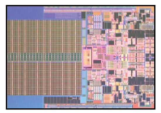
http://images.anandtech.com/reviews/cpu/intel/45nm/penryn.jpg
Last edited by a moderator:
Panajev2001a
Veteran
It could also speed up the loading of new code to the SPUs, which would cut down the stall time of the SPUs when switching programs. Cutting down on that over-head would allow a finer granularity of the tasks assigned to the SPUs and should allow an over all higher efficiency.
How to make SPE's very good at heavy multi-threading/multi-processing swapping contexts in and out rapidly is something that is probably on the minds of a lot of engineers over at STI's labs. Hanging over their heads is the idea that SPE's LS in future CBEA implementations might increase (and so COULD the register file): all of this means that saving out to external memory and then reloading the context into its LS gets more difficult to realize.
If you look in the CBEA docs a L1 cache shared by all SPE's is something that was in STI's mind since well before PS3 ever came out and something which I expect them to constantly work at, but you have to wonder what are the implications of adding caching to the SPE's direct access to memory through their DMA engines.
What would be the right size of such a cache ?
Would a single layer of cache be enough ?
How much does it cost to you to handle and route both MFC's dma accesses passing through the cache and bypassing the caches (you still have to keep programmer's interface between SPE and memory [LS and external] the same) ?
Programmers must be allowed to work as they would with the "older CELL architecture" really bypassing the cache mechanism when they so choose IMHO: if you cannot bypass the cache you would basically have to work as if you had two layers of Local Storage and micro-manage both to also avoid expensive cache misses and destructive interference from other SPE's.
Still, the L1 caches thought for the SPE's did not seem to be concerned with allowing SPE's to quickly and efficiently swap contexts repeatedly over time.
Think about SPE's with say 256x128 bits registers and 256-512 KB of LS: that's a already 260-516 KB of data to be swapped by a single SPE each time it changes context. For 16 SPE's, we are talking about 4-8 MB.
Putting an additional pool 4-8 MB of cache (even e-DRAM based, and assuming IBM's SOI solution is up to the task when used on the field for a high volume processor like Sony needs for is PlayStation line) is not exactly free in terms of die area even at 45 nm (given IBM's own number), especially considering that 16 super-SPE's
(as described above), one or more improved PPE (with likely bigger L1 and L2 caches)In this area, x86 and in general architectures not based on Local Storage (which is part of the thread's context) have an advantage: if STI wants to improve that aspect of the architecture the partner to look at would be nVIDIA (or ATI). Managing that many active threads as they do is certainly a feat to be praised for.
I was actually not thinking about thread switching, instead I had finite tasks which were allowed to run to completion in mind and the switching between such tasks.
However, I understand that thread switching is more powerful and flexible way to control and distribute the computational power in a multi-tasking environment.
I was actually myself wondering how a common cache for the SPUs should be designed. I would like to split in to two parts, one part that caches reads from memory blocks marked as static read-only data (i.e. code, static tables and such, that would allow them to always have the most commonly used SPU code easily accessable) and one part that caches reads/writes to other memory areas. The SPUs should of course have DMA instructions that let them by pass the cache to avoid clogging up the cache with huge amounts of streamed data, (double and tripple buffers will handle the latency of the streamed data anyways).
Switching threads is indeed a pain, if it could be avoided all together it would be the best case, the second best option as I see it would be to request the task to save its own state and yield to a new thread, in that case the thread could save a minimum amount of state information at some suitable place in its path of execution before exiting.
If the thread does not respond to the request within a certain time, the OS could do a brute force swap of the thread and save the necessary information to the stack/cache. If the SPU tasks are properly defined with a code area and a data area, only the registerfile and the data area needs to be stored, no need to store the static code.
Depending on how large part of the LS that is used for data, the amount of state information that needs to be stored could greatly vary for each thread that gets swapped out. Perhaps we could do with less than 4-8 MB for 16 SPUs, but it also depends on how many threads we are juggling simultanously, it´s all pie-in-the-sky numbers, but as long as the amount of state data stay within the cache size it will probably be pretty efficient.
I am not sure IBM wants to introduce a thread switching model for the SPEs, but instead maybe they go for a model where the OS will statically reserve a number of SPUs/process and have some dynamic pool of the remaining SPUs which can be shared, it all depends on the application, number of SPUs, cache size etc. how this could be implemented, there are so many options. :smile:
Last edited by a moderator:
Megadrive1988
Veteran
as far as EDRAM in CELL, didn't some of the older patents from 2002-2003 sugguest that upto 64 MB EDRAM be used per CELL processor? IIRC, then an MCM package of 4 CELLs could have 256 MB. my memory is a bit fuzzy now. Sure that was massively, overally ambitious for the time, even projecting 65nm, and even more out of reach on 90nm.
Yet perhaps true 2nd-gen or 3rd-gen CELL processors will have this, on 32nm in time for PS4 in ~2012 ?
Yet perhaps true 2nd-gen or 3rd-gen CELL processors will have this, on 32nm in time for PS4 in ~2012 ?
Megadrive1988
Veteran
Gosh is it time already, here we go again.
I think the next Playstation will launch sometime in 2015-2016. Sony will probably want to target at least 1080p. Maybe 4k by 4k digital cinema resolution. I doubt they'll abandon Cell or NV, with all the software they will have to invest this generation.
So it will be something like this
Cell2 with 4-8 PPU and 32-64 SPU
SPU local store upgrade to 1-2 MB.
Using 32nm node for 220mm^2 area.
clockspeed around 4 GHz.
paired with 8 GB of RAM with 200+ GB/s bandwidth.
RSX2 base on G160 or whatever they call it.
with between 256 - 1024 MB of RAM with 200+GB/s
20-60 TB of storage
Next Gen Optical with 0.5 - 1TB capacity.
I hope they bring out some cool technology like hologram or something.
2015-2016 is much too late to launch PS4. by that time, Sony will be developing PS5. I don't think the PS4 is going to come out more than 6 or 7 years after PS3. It should not be coming 9-10 years after PS3. no way IMO. not unless Sony wants to place PS4 against NEXT-NEXT gen XBox4, lol!
As for resolution, not a pixel more than 1080p, please. we don't need higher resolutions. we need better graphics and higher framerates. honestly (tho this isn't going to happen) realtime graphics could be produced at 480p that blow away current X360/PS3 graphics that are done in 720p, 1080i, 1080p. I mean NEXT-gen graphics at 480p given enough of an increase in geometry, shader operations, lighting, effects, etc. over the current HD graphics being pumped out by X360/PS3. resolution is nice, but highly overrated and hurts advancement in graphics.
I know the industry is not ever going to go backward, HD resolutions are here to stay, but we don't need anything beyond 1080p and even that is overkill given the fact it takes away from graphics performance. going beyond 1080p for next gen would be just like using 1080p this gen, cutting back severely on what can be put into the actual graphics.
I DO however like the general specs you're coming up with for a next-gen CELL and next-gen RSX though
RenegadeRocks
Legend
Weren't we soppose to have like 3 cells in a ps3 earlier! It would have been awesome and would have ripped the competition apart! It was only when theyactually released the final specs that I realised that there's only 1 cell proc in it, M y friend was completely shocked, as he is a programmer and used to keep telling me how powerful the next PS is gonna be, while we played on our PS2! How did things get so out of hand ( money wise I guess) that their projection of having 3 cells turned to just one?
It would have been awesome and would have ripped the competition apart!
No it would not!
How did things get so out of hand ( money wise I guess) that their projection of having 3 cells turned to just one?
Programming flexibility and perfomance?
There are things a GPU does much better than the Cell.
Megadrive1988
Veteran
Weren't we soppose to have like 3 cells in a ps3 earlier! It would have been awesome and would have ripped the competition apart! It was only when theyactually released the final specs that I realised that there's only 1 cell proc in it, M y friend was completely shocked, as he is a programmer and used to keep telling me how powerful the next PS is gonna be, while we played on our PS2! How did things get so out of hand ( money wise I guess) that their projection of having 3 cells turned to just one?
this is a point of confusion and even I am not 100% clear on it.
IIRC:
one plan for PS3 suggested a CELL CPU with 4 CELLs on one chip, the Broadband Engine (4 PPEs, 32 APUs). then a seperate conventional (Toshiba?) GPU.
another plan suggested 2 or 3 CELLs to handle everything. whether these were on one chip or seperate chips isn't clear.
yet another showed that same 4-CELL CPU (Broadband Engine) plus a seperate GPU with another 4 CELLs combined with rasterizing elements (Visualizer).
deathkiller
Newcomer
That was an hypothesis based in a very early (2001?) announcement of 1TFlops for the PS3 mixed with the announcement that the final Cell would have 256GFlops (2005?). Sony never suggested that the PS3 would have multiple Cell.one plan for PS3 suggested a CELL CPU with 4 CELLs on one chip, the Broadband Engine (4 PPEs, 32 APUs). then a seperate conventional (Toshiba?) GPU.
Similar threads
- Replies
- 5
- Views
- 245
- Replies
- 21
- Views
- 1K