AMD RDNA3 Specifications Discussion Thread

They did not, though. SLI had numerous issues even with the games it worked with. Regardless it wasn't a viable option anymore with how modern engines were architected.

I owned every 'dual core' single PCB GPU ever made and rarely had an issue.

And they wer nearly always striped down cores.
 
P.S. Wave64 single-cycle execution implies that both the lower and upper halves are co-issued to the dual-issue 32-lane hardware. This is contrary to RDNA 2 issuing the same Wave64 instruction over 2 cycles to single-issue 32-lane hardware (hence 2-cycle execution, 1 for lower, 1 for upper).
What do we know about wave size for compute shaders? Some people assume it's 32, others 64.
Afaik the compiler decides arbitraily in a black box, but not sure to which shader stages this applies.
 
More attention was paid to optimizing critical paths, deeper
There's more to it than that, 28nm CPUs clocked twice as fast as 28nm GPUs too.
What they really mean is that for this specific design, that may be the process node limit; you end up being limited by certain critical paths inside the design that can't run at a higher frequency.

Easy way to think about it is Intel's new Alder Lake and Raptor Lake CPUs.

The P-Cores and E-Cores are the exact same process, they're even on the same silicon, but the P-Cores top out about 1500mhz higher than the E-cores do, because their architecture was designed with high clock rates as goal #1. More attention was paid to optimizing critical paths, deeper pipelining, choosing leakier transistors with higher drive strength that can switch faster, but burn more power, etc.

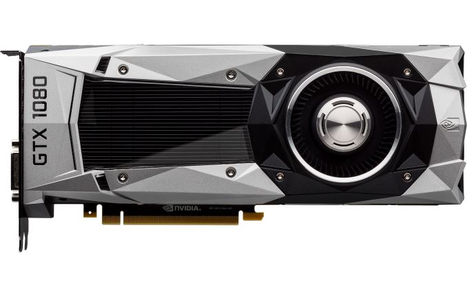
You can also expend a lot of manual effort, both with AI analysis and regular old humans trying to optimize the critical paths in the chip. Not to muddy the discussion too much by mentioning team green, but Anandtech's Pascal article goes into some pretty good detail of how careful design lets you run up the clocks on the same process:

Nothing to be done about it now after the fact though, the design is set in stone and the silicon is out in the wild.
I got it, don´t worry, but then it´s more architecture design limit than manufacture node limit itself as you described by P-core and E-core example. And I had an impression that AMD said RDNA3 is designed with high clockspeed design .
 
Last edited:
What do you mean?
There's something odd about this thing and you'll find out what in due time.
There's more to come?
Seems so.
AMD's Frank Azor is openly talking in this vid how 7900XT/XTX are direct competitors to RTX 4080.
Always were.
The design target was to build something in 400mm^2 cost class rather than the usual 600mm^2 flagship which isn't particularly viable on N5.
 
I think to get reflections of reflections we would approximate the 2nd bounce reflection with a lookup into whatever we use for irradiance cache, e.g. RTXGI probes.
I'd do this also for the full raytraced approach, because recursion is just crazy for realtime, imo. I mean, no matter what, you have to clamp recursion depth anyway at some point.
So i don't think that's a good argument regarding planar vs. RT reflections.

The better argument is simply: If we use HW RT at all, we already accepted the cost of maintainign BVH, so ofc. we will use RT reflections but no planar restrictions. Nobody will mix planar reflections with RT AO, for example.
But if HW RT can't be used, planar reflections and multi view rasterization in general remains a topic.
Even with HW RT on, multi view raster is still used everywhere for shadow maps. Only after HW RT becomes practical enough to get rid of that, the debatte would be settled.

Crysis Remastered already uses a mix. For water the advantage is relatively cheap high resolution reflections vs the amount of rays you'd have to cast, and you can't do temporal accumulation too well as perspective shift and animation ruin both easily for water.

If you can get your planar reflection work ok with RT then it still has a place for relatively flat water bodies just like it's mostly been used for before, you don't really need to think about material response there.
 

Heavily binned die, or a straight up arch failure? A bad cache hierarchy could see the ALUs starved, and looking at it the perf to ALU ratio has widened already.

Could be that RDNA3 here is a bad arch, they went too wide on ALUs, and maybe Navi 32 is an improvement.

But that doesn't make sense for not being able to overclock, even if the resource ratio is bad brute force should still work. Maybe it really is a heavily binned die.
 
I got it, don´t worry, but then it´s more architecture design limit than manufacture node limit itself as you described by P-core and E-core example. And I had an impression that AMD said RDNA3 is designed with high clockspeed design .

Not necessarily, they are both different halves of the same coin.
Architecture X will run into a certain frequency limit on process Y, but change either of the two and there's room for improvement.
Most fabs offer 'enhanced' versions of certain nodes that clock higher and perform better, even with the same or nearly the same architectural design.

AMD could for example expend some work to port the RDNA3 GCD to TSMC N4P, which is largely an optical shrink of their N5 node with similar design rules. Costs you both for the extra engineering effort and in the higher wafer costs, but straightforward to do, even with the same design and architecture. Who knows, that may be already in the works for 7950XTXTX? :)


This is exactly as they did with the basic RDNA2 design and Navi 24, porting it from the basic TSMC 7nm process to 6nm, which was also a very mild optical shrink.

As Navi 24 was a mobile focused design they probably were more interested in the slight reduction in power consumption and area than anything else, but it does clock quite high, the limits in the drivers seems to be the limiting factor:

 
I don't know how many were sold, but it looks like the R9 295X2 used 2 8pin connectors to draw 500W. So there is precedence for AMD drawing more than the 375W "allowed" by the spec.

That might be ok if people are aware of it in relation to PSUs and before they specified this in detail in 2018. The R9 is from 2014 so during the wild west period.
 
Not necessarily, they are both different halves of the same coin.
Architecture X will run into a certain frequency limit on process Y, but change either of the two and there's room for improvement.
Most fabs offer 'enhanced' versions of certain nodes that clock higher and perform better, even with the same or nearly the same architectural design.

AMD could for example expend some work to port the RDNA3 GCD to TSMC N4P, which is largely an optical shrink of their N5 node with similar design rules. Costs you both for the extra engineering effort and in the higher wafer costs, but straightforward to do, even with the same design and architecture. Who knows, that may be already in the works for 7950XTXTX? :)


This is exactly as they did with the basic RDNA2 design and Navi 24, porting it from the basic TSMC 7nm process to 6nm, which was also a very mild optical shrink.

As Navi 24 was a mobile focused design they probably were more interested in the slight reduction in power consumption and area than anything else, but it does clock quite high, the limits in the drivers seems to be the limiting factor:


makes no sense to me, if 5nm node limits RDNA3 arch somehow and could be solved by porting the chip to 4N , why did not AMD choose 4N process in first place ? I think this is just false assumption, just like that porting Vega 64 to 7nm will solve GCN limitations and make it better gaming GPU ...
 
There is no reason to treat any Coreteks claim as credible.

I'm open to the idea that these Navi 31 cards dont have a load of overclocking potential, but I would not take anything Coreteks claims as some confirmation of anything.
 
No.
The reality is a lot funnier than that.

Letsa call it 7970XTX 3GHz edition and throw nostalgiabuxx at the screen.

:(

Wonder how Navi 32 will do. Let's see, die size should be, 200mm for n5, 4x 37.5mm for MCDs. BOM $77 + 29 = $106 for the dies, charge $10 for the packaging.

That's less than the, call it a 4070ti? (408012gb) for a roughly equivalent performance(?). I can see AMD selling it for $649 while Nvidia tries charging $800.
 
Last edited:
makes no sense to me, if 5nm node limits RDNA3 arch somehow and could be solved by porting the chip to 4N , why did not AMD choose 4N process in first place ? I think this is just false assumption, just like that porting Vega 64 to 7nm will solve GCN limitations and make it better gaming GPU ...

Higher end nodes cost more, plain and simple, not to mention you need to book your slots for wafers and plan all this a long time in advance.

That's like saying why would AMD only make Navi31's GCD 48 WGPs and not 64 WGPs and ~400mm2? It's not because they aren't capable of engineering such a thing, it's because just like more advanced nodes cost more, more silicon on the same process costs more, and it'll price itself out of the market.

Also funny you use that as a comparison, they did exactly that and it resulted in the Radeon VII, which clocked higher on the same basic Vega architecture.
Due to very early bleeding-edge access to the TSMC 7nm node it also priced itself out of competition as a gaming card.
 
they did exactly that and it resulted in the Radeon VII, which clocked higher on the same basic Vega architecture.
Due to very early bleeding-edge access to the TSMC 7nm node it also priced itself out of competition as a gaming card.
yes , they did and it din´t help Vega to become better gaming GPU, because despite higher clock, the limitations due architectural design choices still remained :) which actually proves my point, that RDNA3 clock is not limited by process node .-) RDNA2 clock up to 2,8GHz on 7nm , I don´t see any valid point from you, why it´should be worse on 5nm node beside some architectural glitches or design flaw....
 
Back
Top