AMD: Pirate Islands (R* 3** series) Speculation/Rumor Thread

I don't think we have a clear comparison between first-gen HBM and DDR3/4.
However, the overall organization of the DRAM hasn't changed, and there were statements to the effect that it's mostly a wash compared to GDDR5.
The PS4 and Xbox One latencies show similar latency contributions from DRAM between DDR3 and GDDR5.
The very large latency contribution that AMD's memory hierarchy has before going to DRAM is something AMD has indicated they are fixing with Zen, so I think it stands a good chance of improving even if HBM is somewhat slower.

Have they really said so explicitly?
 
One AMD's slides touted a new low-latency cache hierarchy.
Current APUs and the consoles particularly don't set a very high bar, so I'm cautiously optimistic.

Right, found it:

AMDZen-640x360.jpg


If I wanted to be mean, I would say that the memory controller could still screw things up and lead to a very high memory latency, but let's give AMD the benefit of the doubt on this one. After all, Zen will first see the light of day on a pure CPU, so that should simplify things somewhat.
 
The very large latency contribution that AMD's memory hierarchy has before going to DRAM is something AMD has indicated they are fixing with Zen, so I think it stands a good chance of improving even if HBM is somewhat slower.
If AMD fixes the on-chip latency in Zen, there will be much bigger perveived difference between DDR/GDDR/HBM. With Jaguar, the difference between GDDR and DDR in latency is minimal. I would hope that HBM is slightly lower latency than the others, because it is so close to the die (same interposer), even if the technology itself adds some cycles. Is there anything pointing to the other direction? Is HBM designed solely for GPUs (to replace GDDR) or has there been mentions about using it on CPUs (to replace DDR4)?
 
Last edited:
If AMD fixes the on-chip latency in Zen, there will be much bigger perveived difference between DDR/GDDR/HBM. With Jaguar, the difference between GDDR and DDR in latency is minimal. I would hope that HBM is slightly lower latency than the others, because it is so close to the die (same interposer), even if the technology itself adds some cycles. Is there anything pointing to the other direction? Is HBM designed solely for GPUs (to replace GDDR) or has there been mentions about using it on CPUs (to replace DDR4)?

I did some googling to confirm my recollection, and with the speed of light giving ~.3 meters per nanosecond and even with copper signaling being at least a third slower, the distance between the chips itself is not a major contributor. Other factors like needing less to drive the signals might save some time, but that is coupled with a bus that is clocked slower.
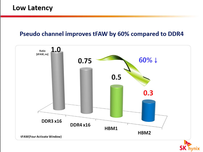
I am trying to find a citation for a rather informal characterization that HBM takes a little longer to deliver the initial part of a burst than GDDR5, but can finish the burst faster.
The raw number of channels can help with loaded latency and increase the CPU's ability to spread accesses over more channels, potentially reducing the number of turnaround penalties incurred.

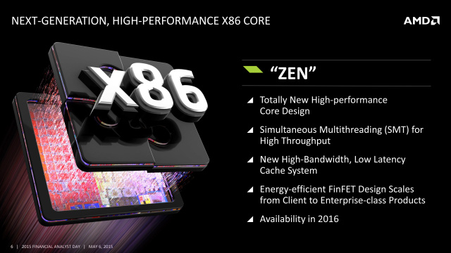
What doesn't necessarily change is the time it takes to fall through the cache hierarchy and traverse the uncore, which AMD hopefully improves.
On the other side, there is the internal logic, routing, and latency of the DRAM arrays.
The arrays have not scaled in latency for years, and DRAM devices have a number of latencies that are measured in wall-clock time, not device speed.

Hynix has marketed HBM for other device types, like networking, but I don't recall a strong push to replace main memory. Perhaps some classes of consumer device can, although WideIO is liked by mobile, and DDR4 will be hard to beat in terms of capacity and pricing.
 
tFAW is generally not what is discussed when the topic is access latency.
That is a device restriction, measured in wall clock time, that is a time window within which at most 4 banks can be activated.
Depending on the access pattern, a CPU could rarely encounter it.
It's not that it can't come up, but it's more of a constraint on sustained bandwidth across banks. Some extra sleight of hand may be needed to map memory locations to take advantage of the pseudo channel mode, so it may not show up the way you'd expect in a memory latency benchmark.
 
Does HBM 256 byte access granularity mean that four adjacent 64 byte cache lines need to be loaded to serve a single cache miss? This would be quite inefficient for random memory accesses (such as hash maps and pointer indirections) that do not even fully use the data of a single 64 byte cache line.
 
Quad-core Zen, with 8xCU IGP and 8~16GB HBM2 on the SoC package, complemented by a speedy M.2 1TB SSD with an option for a second one.
I don't think this makes much sense. I suppose there's a reason there's no option for less than 1024 bits (not cost effective, I assume), and with just a single HBM2 stack, even if they'd stay at the HBM1 frequency/bandwidth the bandwidth would be quite overkill. A Quad-core Zen, with just 8 CUs, would probably be best served with 128bit lpddr4 or something like that if you don't want memory modules (there should be faster lpddr4 out by that time, which would give you about the same bandwidth as the HD 7750 gddr5 had, which should be plenty considering APU gpu clock is typically lower AND it should have framebuffer compression). I suspect that would be cheaper and be very similar in performance overall. Double the amount of CUs (which is quite reasonable for a 14nm chip) and it might make some more sense...
Plus more than 8GB would be plain impossible in that timeframe I believe (unless you want two stacks???) with HBM2.

Halve the Fiji GPU (32 CUs) + add four Zen cores (4 cores = 8 threads) on the same die + 8 GB of 256GB/s HBM2. Would make a perfect high end gaming laptop (with reduced GPU clocks to get better perf/watt). No discrete GPU required.
That'll make some more sense though the amount of memory is imho a bit limiting for a high end gaming laptop for that timeframe. Unless you'd opt for two HBM2 stacks (or just use ordinary ddr4 memory alongside it)...
 
Last edited:
Does HBM 256 byte access granularity mean that four adjacent 64 byte cache lines need to be loaded to serve a single cache miss? This would be quite inefficient for random memory accesses (such as hash maps and pointer indirections) that do not even fully use the data of a single 64 byte cache line.
As a layman I guess you are right.
Timothy Lottes on this subject:
HBM
HBM definitely represents the future of bandwidth scaling for GPUs: a change which brings the memory clocks down and bus width up (512 bytes wide on Fury X vs 48 bytes wide on Titan X). This will have side effects on ideal algorithm design: ideal access granularity gets larger. Things like random access global atomics and random access 16-byte vector load/store operations become much less interesting (bad idea before, worse idea now). Working in LDS with shared atomics, staying in cache, etc, becomes more rewarding.

http://timothylottes.blogspot.de/2015/06/amd-fury-x-aka-fiji-is-beast-of-gpu.html
 
Does HBM 256 byte access granularity mean that four adjacent 64 byte cache lines need to be loaded to serve a single cache miss?
I was told each 1024 bit stack is divided into 8 channels and the burst length to be 2 or 4. So isn't the access granularity 32 or 64 bytes?
 
Does HBM 256 byte access granularity mean that four adjacent 64 byte cache lines need to be loaded to serve a single cache miss? This would be quite inefficient for random memory accesses (such as hash maps and pointer indirections) that do not even fully use the data of a single 64 byte cache line.

I don't think that figure is correct.
The standard indicates that all channels should be independent, and the granularity for that is 128 bits with a burst length of 2 or 4.
The larger number seems to be adding together the bursts for all the channels in a stack. If there is something going on the the other side of the interface, that is one thing, but HBM's granularity is smaller than 256 bytes.
 
Does HBM 256 byte access granularity mean that four adjacent 64 byte cache lines need to be loaded to serve a single cache miss? This would be quite inefficient for random memory accesses (such as hash maps and pointer indirections) that do not even fully use the data of a single 64 byte cache line.

Infinisearch and 3dilettante are right. HBM stacks each consists of 8 independent channels, that are logically completely separate. Each channel is 128-bit wide, and can require burst length of 2 or 4, so it transfers 32 bytes or 64 bytes per access.

This design seems optimized to match well with the existing AMD GDDR5 memory controllers -- lots of independent links leading to different devices get converted into lots of independent links leading to different channels on a HBM stack.

Btw. How do the HBM2 latencies compare to DDR3/DDR4? CPU part needs low latency.

The primary latency contributions, reading from the DRAM arrays and precharge, are exactly the same as all other modern DRAM. There are some differences, but they are relatively minor compared to the time cost of actually reading from capacitors. So expect just a few percent here and there.

Negative points would be that lower clock rate means that first arrival of signal takes longer, and that the standard lacks "most important word first" feature. Not that it's very important.

Positive would be that having so much more banks spread across so many channels means that in a latency-limited scenario (pointer chasing) with little other load on the system, the odds of hitting a precharged bank with each new load is much higher. Also, wider bus should mean that transfers complete faster than on DDR4.
 
Halve the Fiji GPU (32 CUs) + add four Zen cores (4 cores = 8 threads) on the same die + 8 GB of 256GB/s HBM2. Would make a perfect high end gaming laptop Nintendo NX tablet/home console hybrid.

Fixed that for you!
Ah.. one could only dream..

But it's Nintendo, so I'm going to cry over that corner now :(
 
The larger number seems to be adding together the bursts for all the channels in a stack. If there is something going on the the other side of the interface, that is one thing, but HBM's granularity is smaller than 256 bytes.

This sounds like "ganged" vs. "unganged" in DDR MCs.
 
In power-constrained environments (i.e., everywhere, now) everything that saves power increases performance.
It's incredibly nice that a GTX 970 consumes so little power. It's a major item to put on your marketing material, and it resonates very well with consumers.
But is it something that limits performance? Except for that small sliver of ultra-high-end gaming laptops, not really.
 
If all goes well, the new architecture will go beyond what is realistically achievable with GDDR5 at the high end.
The question is really how much more efficient can be gained beyond Maxwell (adjusted for process, of course.) For gaming workloads, I doubt there's going to be a huge additional jump, though I've been proven wrong about these kinds of claims in the past. So, for now, I'm assuming just process scaling in terms of perf/mm2. Say a 50 to 60% increase per mm2. That gives a 400mm2 chip roughly the same performance as a 600mm2. We already know that a 600mm2 doesn't strictly need HBM to be competitive...

1TB/s bandwidth is going to be possible within 18 months. There's no way to build a single chip GPU with GDDR5 that's going to hit that bandwidth.
Of course. Nobody has made such claim.
 
AMD targeted only the enthusiast segment for HBM (q2 2015 financial conference call) so I think HBM 2 will only be for the next gen high end and HBM gen 1 for mid range and lower end GPU's. It really doesn't make sense with the extra cost and bandwidth of HBM 2 to go to lower than the enthusiast SKU's.

They didn't answer the HBM vs older model's margins based for ram I think we can take that its much more expensive.......

Oh they stated they have a lead time for HBM already, but they didn't answer how long and how they are taking advantage of that, so how we look at that.......
 
Last edited:
HBM gen 1 won't be any cheaper than HBM gen 2. Actually, for lower end devices that need more memory than 1GB yet don't necessarily need the BW of many stacks HBM2 could be cheaper.
 
Back
Top