Will there be GDDR 6 ??

iwod

Newcomer
I have seen rumors or some BS about GDDR 6, but i have yet heard anything from Nvidia, ATI, or JEDEC,
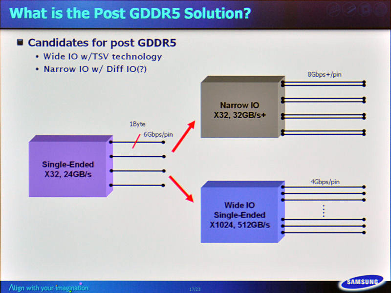
Since we dont want 512 bit memory lane ( because it is too expensive ), 256bit Memory will hit an wall sooner or later. Do we expect GDDR 5 to scale even further? Or We ditching GDDR5 for something else?
 
AMDs London mobile 28nm GPU family is rumored to have a 192-bit member. So we might see 320- or 384-bit in high-end.

GDDR5 was planed to scale to 7Gbps with low-voltages, after this Samsung planed Next-GDDR: http://translate.google.ch/translat...19593.html?ref=rss&sl=ja&tl=en&hl=de&ie=UTF-8

ph09.jpg
 
There used to be a presentation from Qimonda talking about what could come next after GDDR5, a stack of DRAM chips with TSVs buried beneath the main IC inside the chip package was IMO the most promising approach.

As the image above says, regardless of what you do with the interface technology ... if the signal has to go across a PCB you just can't approach what you can do with stacked area I/O MCMs, XDR is not the answer ... it's a stopgap at best which might give a couple 10% boost in bandwidth (power consumption savings will be greater though).
 
Arh,... thanks... i think it was Wide IO with TSV that Samsung just announced not too long ago....
At least for DRAM.... So i think GDDR NG will be heading that direction due to cost incentives...
 
Won't cooling be hell of an issue with DRAMs stacked on the GPU ASIC? Or if you stack the DRAMs on the circuit side of the die, how do you route I/O to the GPU? Seems a difficult proposition in a high-end product. Naturally, for cool-running low power devices it won't be an issue, but then you don't need stacking for performance scaling anyway. Then you just do it to conserve space and power...
 
The DRAM doesn't create that much heat, just put Cu planes in between the DRAM dies and connect those to a small heatpipe to the top of the package and the main heatsink.
 
The DRAM doesn't create that much heat, just put Cu planes in between the DRAM dies and connect those to a small heatpipe to the top of the package and the main heatsink.
What Grall is saying makes sense, though. Are you saying for the GPU to be on the PCB side of the stack or the HS side? If the former, then I doubt copper planes can do as well as direct contact with the HS for cooling the GPU. If the latter, then TSVs have to pass GPU I/O and power through the DRAM chips.
 
OIC what you mean ... but the DRAMs are relatively thin, so the resistance/inductance of TSVs carrying power doesn't necessarily have to be a factor (after DRAM is out of the way the remaining I/O is almost irrelevant). You'd probably put alternating ground/power planes in between the DRAMs.
 
Last edited by a moderator:
I just thought why cant TSV be applied to SRAM? Hypothetically, you could have layers of SRAM and Memory Controller, Which would give something like 32MB L3 Cache on CPU and GPU.
 
3D ICs will change a whole lot of design practices, and it might indeed be profitable to put caches on a different plane ... that's far future stuff though. A DRAM stack under the IC hopefully a little less so.
 
Why is 512bit such a big problem ? 8 memory chips on each side of the PCB, at least for the fastest cards. When they can sell monsters like gtx590 for 700$.
 
They don't even say if it's single or double-ended. :LOL: For something that's supposedly coming out in two-something-two-and-a-half maybe years, they sure are secretive. Surely, these decisions have already been made by now?
 
Back
Top