AMD: R8xx Speculation

How soon will Nvidia respond with GT300 to upcoming ATI-RV870 lineup GPUs

  • Within 1 or 2 weeks

    Votes: 1 0.6%
  • Within a month

    Votes: 5 3.2%
  • Within couple months

    Votes: 28 18.1%
  • Very late this year

    Votes: 52 33.5%
  • Not until next year

    Votes: 69 44.5%

  • Total voters
    155
  • Poll closed .
USD 349 ---> Rip off :cry:

"BOM" of every add-in card(5800 series) may be within the region of 120~150 USD.

BOM has little to do with retail price. If the customer is willing to pay a price, the vendor will sell at that price. If no one buys @ $349 prices will come down.

Just be glad there is competition and we're not paying the $600+ Nvidia's been so happy to charge for their top-bin parts oh so many times. 7800 GTX 512 anyone? Remember the GT200 launch? GTX 280 was $650 until HD4xxx was announced and NV had to slash prices across the board to have any chance of selling product until they could get the 285/295 out the door. Remember $450 GTX 260s? I bought one (for a customer) for $150 a couple weeks ago.
 
with the Geforce 295 still at $500, you're getting that level of performance for $300/$350.. everyone should be a happy camper.
 
BOM has little to do with retail price. If the customer is willing to pay a price, the vendor will sell at that price. If no one buys @ $349 prices will come down.

Just be glad there is competition and we're not paying the $600+ Nvidia's been so happy to charge for their top-bin parts oh so many times. 7800 GTX 512 anyone? Remember the GT200 launch? GTX 280 was $650 until HD4xxx was announced and NV had to slash prices across the board to have any chance of selling product until they could get the 285/295 out the door. Remember $450 GTX 260s? I bought one (for a customer) for $150 a couple weeks ago.

I saw the gtx 260 for $125 recently btw. Competition is great.
 
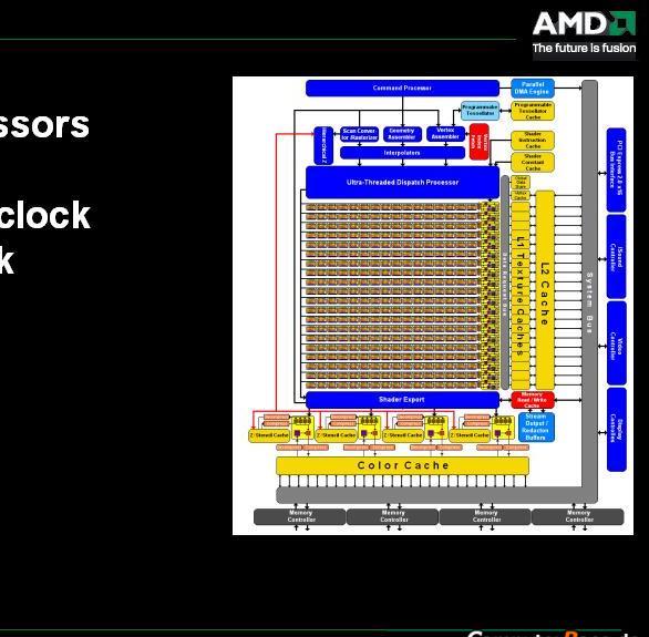
This card sports a 2nd gen TeraScale engine that delivers more than 2 teraFLOPS of processing power

Hmm, to reach 2T you can do

1280(alu's) *2(fma)*781MHz,
1600(alu's)*2(fma)*625MHz,

Since rv770 already runs at 750MHz, the new shder count seems to be 16 SIMD's, downright tepid compared to rv670->rv770 transition.

And then there is of course the question of what are they doing with the ~350mm2 die area?
 
How can you answer the last question even with speculative math when you don't know how much the X11 requirements consume in the first place?
 
My point was that the increase in flops (and the associated increase in tex, rops, alu,tex,rop ratio assumed static of course) is too low to fill up 350 mm2 worth of area. I can only assume that it must be taking up a lot of area, because otherwise we'd prolly have seen a larger increase in alu's and texturing.
 
My point was that the increase in flops (and the associated increase in tex, rops, alu,tex,rop ratio assumed static of course) is too low to fill up 350 mm2 worth of area. I can only assume that it must be taking up a lot of area, because otherwise we'd prolly have seen a larger increase in alu's and texturing.

I think that this time the HD5850 will have less SP than the HD5870: both will have GDDR5, so I don't think that different memory clocks would be enough to differentiate them...
So I assume around 1300SP for the HD5850 and 1600SP for the HD5870: the diagram seems quite clear, and realistic, too.
1600 different SPs (in order to process the new shaders), 80TMU, a brand new scheduler and a new bus (no hub) are enough for 350mm2, don't you think? ;)
Sounds ridiculous...
 
How can you answer the last question even with speculative math when you don't know how much the X11 requirements consume in the first place?
I think we have a view... If we consider RV830 / 180mm² to be 640SPs part, then a GPU, which has almost double die-area (so likely twice as much transistors, +90-95%), shouldn't be based on 1280SPs.

RV350 - R350: 2x ROPs/TMUs/ALUs/bus => +50%
RV410 - R420: 2x ROPs/TMUs/ALUs/bus => +33%
RV530 - RV570: 3x ROPs/TMUs/ALUs, 2x bus => +120%
RV630 - RV670: 4x ROPs, 2.7x ALUs, 2x TMUs/bus => +70%
RV730 - RV740: 2x ROPs/ALUs, + GDDR5, + DP support => +60%
RV730 - RV770: 2x ROPs, 2.5x ALUs, 2x bus (+GDDR5), +DP support => +85%

I'd say with +50-60% (280-290mm²) doubling of almost every functional part of the GPU should be possible. For a 90% bigger GPU I'd expect something like 2x ROPs/bus, 2.5x ALUs/TMUs.

If RV830 has 640 SPs, than 1600 SPs (2.5x) seems to be in the range of possible configurations for RV870 (350mm²). If RV830 will have 800 SPs, I wouldn't be surprised by 2000 SPs for ~350mm² GPU.

Yes, we don't know how costly the DX11 implementation is or how many SPs does the RV830 have. But we know size ratio of two dies, so we can base the estimation upon proporcional difference.
 
I think that this time the HD5850 will have less SP than the HD5870: both will have GDDR5, so I don't think that different memory clocks would be enough to differentiate them...

I guess they'll be differentiated by clocks and number of power connectors - ie 5850 will be clocked low enough to be running with just one 6 pin - which would limits it's OC potential from getting to 5870'ish speed.
 
What, to have a "crippled" gpu for a lower level version of a card? Wasn't it what ATI did up to some time ago and NVidia continues to do still now (the GT200 in GTX260, for example)? ;)

4830/4850/4870?

The 5850 won't be a crippled part, but a speed binned part. Expect a 5830 as a salvage part.
 
Back
Top