R700 Inter-GPU Connection Discussion

Arty

KEPLER
Veteran
I can't see why you'd need a chip between the two gpus? What's the point? Sure just as the normal pcie bridge (instead of the old pcie 1 one) this will do fine - 3 ports would be enough, however (communication is only 3-way...)
Here is R700: http://img.hexus.net/v2/graphics_cards/ati/4850X/R7001-big.jpg

Look carefully between the two gpus. Its definitely there, looks smaller too. Also notice the arrangement of the components arranged horizontally between the two gpus in R680 and it is arranged vertically on the R700.

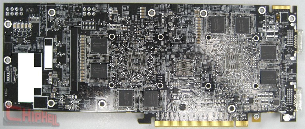
R680 (Back): http://www.techpowerup.com/reviews/HIS/HD_3870_X2/images/back.jpg
R680 (back with metal plate): http://www.techpowerup.com/reviews/HIS/HD_3870_X2/images/card3.jpg
R680 (front): http://www.techpowerup.com/reviews/HIS/HD_3870_X2/images/gpus.jpg
 
2008062821e8649056b17c3ba0.jpg


Still PLX and probadly they have to use the 12 port device, since PLX does not offer something other.
 
Maybe we need a R700 speculation thread now :devilish:

Chiphell seems to have the pcb shots of the R700 now. Black pcb and all...

Chiphell
2617130103_da0ab5f6de_b.jpg

2617131693_5ddd77d49b_b.jpg


No surprise there as we see the smaller PCIE 2.0 PLX chip. Also of note is that the board is definitely much shorter than the R680 it looks like. RAM is on both sides as well.

Then there was this CNET article today that mentions the new propietary interconnect.

CNET Article

For ATI, the execution of this chip-ganging strategy is the key. And this is where ATI appears to have been successful. "The inter-processor communications. Getting that to work has been the trick. This is what ATI has done. They've come up with this stellar way of doing inter-processor communications so they can in fact get the scaling," according to Peddie.

AMD-ATI's upcoming R700 (rumored to be called the 4870 X2) two-chip graphics board will be the ultimate test of this strategy.

"It's a new proprietary inter-processor communication technology. If they put these two chips on one board and it does scale properly, then they have pulled off a coup," he said.

"When you gang up graphics chips (using the traditional Scalable Link Interface or CrossFire technologies) they roll off pretty fast. ("Roll off" implies that performance doesn't scale up well.) "So when you put two boards in, you don't get twice the performance but you (only) get one and a half. You put four boards in and you (only) get about 1.7, 1.8. What ATI is saying is that with two chips using (their) proprietary inter-bus, they will get 1.8 (the performance) with two chips. If that's true, you can expect to see four of them giving you something around 2.5."

Getting 2.5 times the performance from four boards would be a masterstroke for ATI.

The previous ATI dual-chip solution was very different, Peddie said. "The HD 3870 X2 was not a proprietary bus but a CrossFire connection. The CrossFire connection and the SLI connection are at the very, very end of the pipeline. Not the most efficient place to do an inter-processor communication. That's one of the reasons ATI has abandoned it."

So basically the card will not be CF on a board but will be a new interconnect between the GPU's. Also, it seems to suggest that the CrossFire connection was redone in the RV770 or at least for R700 since Peddie suggests that the CF connection is no longer at the very very end of the pipeline. Maybe that's why recent CF results of the 4800's show incredible scaling when it works?

Anyways, with the plethora of information of R700 that was just released it seems like ATI is pushing hard to get these cards out fast.

This sounds very promising! They still need to ensure all games are supported though and that gamers don't have to wait for new profiles before a game will scale. Then there is the issue of micro stuttering to eliminate. If this new solution can solve bth of those issues then I might even consider a switch!
 
Thanx for the feedback guy's :)

Wow that X2 PCB looks sexy, I read somewhere in an ATI slide CFX with two X2's would scale as good as 3,75 (as 2 GPU's afa scaling is conserned)
 
Looks like the board is equipped with GDDR5 memory as the chips are slightly squarer than the GDDR3 chips on HD4850. Qimonda memory appears to be on all RV770 boards.

Jawed
 
Depends on the partner. ;)

Dave, you're implying that AMD allows free reign over the flagship card PCB designs? :eek:

Closest I've seen is the Powercolor GDDR4 3870X2, but that could have been a one-off.

Now that's a pretty radical step compared to the other opposing IHV. Not that someone would make custom PCBs for costdowning their flagships though.
 
I'm guessing it will be around 10 GB/s, enough to get smoother replication of textures for AFR ... not enough to texture from remote memory on the fly.
 
Maybe we need a R700 speculation thread now :devilish:

Well, at least one to discuss this new interconnect. And now we have one.

So basically the card will not be CF on a board but will be a new interconnect between the GPU's.

Choosing to call such a setup "R700" obviously makes the heavy implication that there is perfect transparency to the user, doesn't it? I guess we'll see, but my first thought is that goal will only be approached not attained. How close they get will drive my attitude on whether they were well served to use such naming rather than some variant of the "CrossFire" branding so as to promote clarity rather than confusion.

This sounds very promising! They still need to ensure all games are supported though and that gamers don't have to wait for new profiles before a game will scale. Then there is the issue of micro stuttering to eliminate. If this new solution can solve bth of those issues then I might even consider a switch!

Yes, this is going to be the key. Does it still require profiles? If so, how are those profiles created and distributed?

It occurred to me recently that if profiles are still required that I don't even really care if AMD provides an editor. . . . my minimum position is that they bust them out of the driver .dlls into their own unencrypted file(s) in the driver package. Why? Because then they can be reverse engineered and third party profile editors created by the enthusiast community. You know that would happen if AMD wasn't actively making it impossible.

Not that I object to AMD writing their own profile editor. But if resources are a big issue here (which is what the quote from Terry in my sig suggests) and they can't lead or follow at the current time on a profile editor, then just at least get out of the way. . . .
 
Maybe someone has an idea, how the sideport memory could be related to R700s new interconnect, as some rumors said, which I heard. ;)
 
OK, let's get wild now! If the mentioned "sideport" is just a second PCIe switch in every RV770, would it be possible to do CF-on-a-stick setup, without the PLX bridge (at some performance cost)? :oops:
 
OK, let's get wild now! If the mentioned "sideport" is just a second PCIe switch in every RV770, would it be possible to do CF-on-a-stick setup, without the PLX bridge (at some performance cost)? :oops:
The PLX brdige will be needed everytime, no matter how the GPUs communicate with each other, it's main function is to connect the 2 GPUs to the rest of the system, if they were to implement that function into the GPU it wouldn't make sense because you'd have the same function on both GPUs and one of them would go to waste. They could just as well have their own interlink paths somewhere beneath the chip and not use the bridge at all for inter-communication, but the bridge is still the only reasonable option to talk to the PCIe port.
 
Depends on the partner. ;)
So some partners could still use the Gen1 PLX bridge? If thats the case, wonder what the performance penalty would be like.

The second possibility is that they could design their own bridge .. dont know if thats possible. :unsure:

The last possibility is that there could be no bridge required at all .. but then why would the protos have one?:sly:

I think he means that since AMD is such a large partner, they have access to PLX chips that are not (yet) publicly known.
 
I think he means that since AMD is such a large partner, they have access to PLX chips that are not (yet) publicly known.
The Gen2 PLX bridges were announced last year and are in production now. If the bridge in question is something else, we would have to wait quite a bit.

Its most definitely a 27mmx27mm (used my screen calipers :LOL:); so its either 8648 or 8647 (not listed). Note that 8647 has only 3 ports, which is why I asked if these ports hold any significance for the new CrossFire sideport.

And this:

156tg05.png


More:
http://i29.tinypic.com/2mnestj.png
http://i31.tinypic.com/2qwd9c5.png
http://i30.tinypic.com/2v1suwy.png
 
Back
Top