
Significant IP blocks are developed in TO and contribute to just about every ASIC.
You are using an out of date browser. It may not display this or other websites correctly.
You should upgrade or use an alternative browser.
You should upgrade or use an alternative browser.
AMD: R7xx Speculation
- Thread starter Unknown Soldier
- Start date
- Status
- Not open for further replies.
[...]
=>w0mbat: The RV770 doesn't have a ring-bus? You sure of it?
Yes, im quiet shure.
http://eetimes.com/news/latest/show...XITDCIQSNDLRSKH0CJUNN2JVN?articleID=208404063
Seems to me this was a decision made before AMD came on the scene.
AMD hasn't chosen to stop making halo graphics cards - it's decided to make them with 2 GPU chips.
Jawed
So they're saying ATI made this decision roughly just after R580? That's interesting. That would be after the discussions with AMD began (Dec 2005), tho before they were consummated (July 2006). And possibly nearly simultaneous with when the decision was made to go forward with the AMD marriage.
Remember the AMD/ATI merger briefing docs and the pics of the multiple gpu boxes for high end and whether that meant anything for real or was a representation of x performance?
It's quite possible that ATI can make a 4870x2 to take the performance crown (and do it cheaper, cooler and with less power than it's monolithic competiton), while Nvidia simply can't make a G280x2. Right there you can see the advantages of going multicore demonstrated in the form of a product that's viable verses a product that isn't.
ATI decided to get out of that dead-end early (and paid for it over the last couple of chip generations) while Nvidia tried to stick it out with monolithics for as long as possible - but it's put them behind on their next steps towards multi-GPU.
Well, ATI had a lot of catching up to do with multi-gpu. About two years worth, probably. They seem to have largely done it now tho. Altho. . aren't we still waiting for the profile editor that Terry finally conceded they needed about 18 months ago?
Tho personally I've yet to dip toes in that water, and there are still considerable downsides to multi-gpu, some of which likely won't ever be entirely conquered.
Any guess, where should be that CF port, looking at the die shot?
My guess: not in the center
") .
.Seriously though I can't spot much on that die shot apart from the 10 shader clusters - where are the 4 rop blocks, for instance?
Even the shader clusters remain mysterious: seems to me there are 4 blocks (with 4 vec5 alus) starting from the right (lighter areas are cache? Register file?) Then comes another smaller block - TF? - followed by another - TA? - and to the left of each cluster (the biggest block) is thread arbiter and stuff?
Hmm....
leoneazzurro
Regular
No more ringbus + fixed performance (by way of lots more units while keeping transistor count fairly low) seems to indicate that the ringbus naysayers were right & the ringbus was a waste of transistors?
Do we know which bit of ATI/AMD designed the RV770?
Team A: R300 -> Xenos -> RV770?
Team B: R420 -> R520 -> R600
is it possible that one RV770 has only "2 ringbus stops" ?
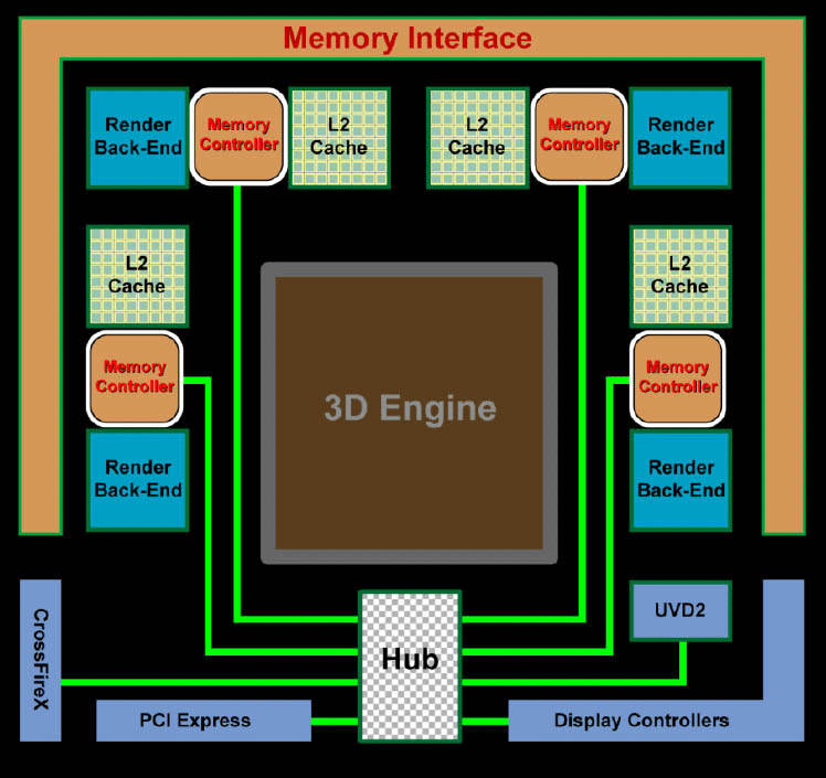
RV770 has no ringbus.
As far as I can tell, there is no more the "ring" but there is the "bus"
So there should be also the bus stops.
PS: I was just thinking that RV770 is in some way a more radical departure from the RV670 architecture than GT200 is from G92... I think it will need a lot of time for the driver time to optimize for it (and they will not be at ease with so many TU at disposal.. maybe they will continue to use only 16 until they will not gain enough practice
)Radeon™ HD 4800 Series Hotfix
The information in this article applies to the following configuration(s):
* Radeon™ HD 4870 series
* Radeon™ HD 4850 series
This Hotfix improves overall performance and stability. The Hotfix includes the Display Driver and Catalyst Control Center.
http://support.ati.com/ics/support/default.asp?deptID=894
Looks good.
Strange - until very recently i was (supposed to be...) under the impression, that a ring bus MC was to deliver a much more efficient memory architecture than an old-fashioned crossbar-controller.Better performance, less space used and now u know how R700 will work. The two RV770 will connect via this new MC.
Remember that most of the time caches in GPUs are there for very different reasons for caches in CPUs. It's more about input/output streaming, latency compensation and bandwidth optimisation. Classic % hit rates just aren't relevant - miss with every access and it will still run at full rate. Reuse tends to be intensely localised (e.g. bilinear filtering reading 4 values and the next texture fetch happening to need 2 of those again) rather than 'now and in 1000 cycles time'. And the cache is sized 'just right' because for a given scenario there is an optimum size above which more makes no difference...effectiveness of the caches
Strange - until very recently i was (supposed to be...) under the impression, that a ring bus MC was to deliver a much more efficient memory architecture than an old-fashioned crossbar-controller.
Yes, cause AMD said so. But theres a reason why the changed it. And i didnt say that it will be old-fashioned
leoneazzurro
Regular
Strange - until very recently i was (supposed to be...) under the impression, that a ring bus MC was to deliver a much more efficient memory architecture than an old-fashioned crossbar-controller.
There is not (only) the crossbar AFAICT there, there is another interconnection bus that has no more the form of a ring, if the diagrams could be trusted.
I heard the reason is that to connect more than 4 SIMD, a ring bus is not very efficient, whereas the new interconnect is.
Remember that most of the time caches in GPUs are there for very different reasons for caches in CPUs. It's more about input/output streaming, latency compensation and bandwidth optimisation. Classic % hit rates just aren't relevant - miss with every access and it will still run at full rate. Reuse tends to be intensely localised (e.g. bilinear filtering reading 4 values and the next texture fetch happening to need 2 of those again) rather than 'now and in 1000 cycles time'. And the cache is sized 'just right' because for a given scenario there is an optimum size above which more makes no difference...
That makes sense.
I guess I was thinking more about GPGPU uses, where the limited size of the individual caches would be more problematic.
Shared lines used for synchronization would be another reason to install a way of tracking sharing.
Mintmaster
Veteran
Now that we have better die shots, I found that the ALUs on RV770 occupy either 28.0% or 25.3% of the die, depending on whether that similar looking sliver next to the left of the 4x10 array is redundancy or not. Feel free to update your numbers.So, RV770's 1200GFLOPs take 104mm2, while GT200's 1000GFLOPs take 153mm2:
For double-precision:
- RV770 is 11.5 GFLOPs/mm2 on 55nm
- GT200 is 6.6 GFLOPs/mm2 on 65nm
Jawed
- RV770 is 2.3 GFLOPs/mm2 on 55nm
- GT200 is 0.5 GFLOPs/mm2 on 65nm
Anyway, a quad of 5x1D units, capable of 20 MAD/cycle, is 1.8 mm2.
An 8x1D SM on GT200, capable of 8 MAD+MUL/cycle, is 5.1 mm2. Maybe 4 mm2 on 55nm.
That's pretty remarkable. Even for serially dependent scalar instructions and 20% efficiency, ATI's ALUs can do as much per clock per mm2. If ATI can figure out how go asynch and double the clock without doubling the size for next gen, we'll be looking at insane computational density.
We're already talking about 100 flops and 2.5 texture accesses per pixel at peak color fillrate.
EDIT:
Bad mistake. I fixed my numbers.
Last edited by a moderator:
Looking at the physical size of the arrays gives me pause.
Which is harder to upclock, the superscalar arrays that span most of the chip's width or pretty much every other portion of it?
Nvidia likely kept their SIMD widths small and the units scalar just for this reason.
Which is harder to upclock, the superscalar arrays that span most of the chip's width or pretty much every other portion of it?
Nvidia likely kept their SIMD widths small and the units scalar just for this reason.
Doesn't look like a redundant part to me. It's similar but clearly different to half-a-quad 5x1D unit (for a start it's less than half the size).Now that we have better die shots, I found that the ALUs on RV770 occupy either 28.0% or 25.3% of the die, depending on whether that similar looking sliver next to the left of the 4x10 array is redundancy or not. Feel free to update your numbers.
shouldn't that be 20 MAD/cycle?Anyway, a quad of 5x1D units, capable of 40 MAD/cycle, is 1.8 mm2.
Well yes but designing the ALUs for twice the clock would surely make them bigger - maybe not quite twice, but by a significant amount.If ATI can figure out how go asynch and double the clock without doubling the size for next gen, we'll be looking at insane computational density.
(As a side note, if you'd compare a 9800GTX+ vs. HD4850 the G92b alus now run at _three_ times the clock of those of the rv770...)
Well yes but designing the ALUs for twice the clock would surely make them bigger - maybe not quite twice, but by a significant amount.
I don't know if the ALUs are the primary problem. It's the control logic and signal distribution.
For reference, Itanium is the widest VLIW chip I can think of, with an issue width of 6 at ~2 GHz.
One SIMD array is equivalent to a sustained issue width of 5 ALUs, 1 branch X 16 =96.
It's not apples to apples, but there's no getting around the fact that 1/10 of RV770's ALU resources is sixteen times as wide as Itanium.
Nvidia's SIMD arrays are much more narrow.
Larrabee, will allegedly have a SIMD unit with much more restricted data flow 1/5 or 1/6 (don't know about the branch unit) as wide.
The SIMD sequencers would probably blow up in size faster.
- Status
- Not open for further replies.
Similar threads
- Replies
- 4
- Views
- 2K
- Replies
- 168
- Views
- 32K
- Replies
- 220
- Views
- 87K
- Replies
- 90
- Views
- 13K